* On your first PCB Assembly order!
* Up to $300 discount
 C - A L L E Y
What is electronics reverse engineering?
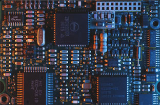
Reverse engineering of printed circuit boards (PCBs) is a technique for dissecting and comprehending the design concepts of an already-existing electronic product. A PCB is disassembled and examined in order to learn about its construction and functionality. Additionally, the procedure aids in developing PCBs with improved features or at a lesser cost. Additionally, this procedure can be used to generate documents for future use.
Reverse engineering offers detailed material descriptions and process knowledge to the semiconductor industry. It falls into four categories. The most fundamental kind of reverse engineering in the electronics industry is product disassembly. This is not how PCB assembly is done at all.
Reverse-Engineering Procedure
1.Creating circuit images by drawing, scanning, or taking photographs.
2.Editing and uploading the images in suitable reverse-engineering software.
3.Replicating the layout design for each layer of the PCB.
4.Generating the circuit schematics using an appropriate tool.
Reverse engineering requires the use of a sample PCB, either populated or bare board. The PCB is initially inspected for mounted components, connectors, and traces on the exterior layers in the reverse-engineering approach. In order to examine the traces and vias in the internal layers, the PCB is later de-layered.
One needs to either take a picture or scan the PCB image. A high resolution should be had by the camera or the scanning device. It is best to take the picture against a dark background in an area with good lighting. This is crucial if the PCB's design is intricate. If the design is straightforward, the circuit can be written by hand using the PCB's precise dimensions. It might be necessary to make additional edits to the image in order to make it compliant with the software used in the following phase.
Component identification, bill of materials (BOM) preparation, technical data collection, and signal analysis are all done physically in manual PCB reverse engineering. This is a laborious procedure that requires prior experience and knowledge.
Why Choose China PCBA Supplier KSPCBA as Your electronics reverse engineering Manufacturer?
– Experienced and skilled team
– State-of-the-art equipment
– Strict quality control
– Excellent customer service
– Competitive price
How can we make high quality PCBA products?
Strict incoming material inspection control and management.
Never change BOM indicated material brand without customer’s permission.
Standard Operation Procedure
PCB will be baked in the oven machine in advance.
Fully automatic, high precision SMT and test equipment.
Comprehensive testing include AOI, X-Ray, ICT, software burning according to different PCBAs.
Strict quality management system.
Please send Email to kspcba@c-alley.com or call us through +86 13828766801 Or submit your inquiry by online form. Please fill out below form and attach your manufacturing files( PCB Gerber files and BOM List) if need quotation. We will contact you shortly.
 +86 13828766801
 kspcba@c-alley.com
 https://www.kingshengpcba.com/
 2/F, Building 6, Tangtou 3rd Industrial Zone, Tangtou Community, Shiyan Town, Baoan District, Shenzhen, China, 518108
We would also like to thank our customers for their trust and support. The company's outstanding achievements are mainly due to the loyalty of our customers, which also encourages and spurs our company to forge ahead.