* On your first PCB Assembly order!
* Up to $300 discount

Product Name GPS PCB Assembly
1.KingshengPCBA Turnkey solution
2.PCB Assembly, PCB/PCBA Design, PCBA Copy
3.Customized PCBA/OEM/ODM/EMS(Electronics Manufacturing Service)
4.SMT&DIP&PTH&BGA Assembly
5.Component sourcing and purchasing
6.Quick PCBA prototyping
7.Test:X-Ray,AOI,In-Circuit Test(ICT),Functional Test(FCT)
GPS PCB Assembly Description
The era of lengthy GPS navigators is over, owing to the quick advancement of electronic technology. Because of this, you can't depend on the big GPS navigators to give you directions like your grandfathers did decades ago. Instead, adding GPS functionality to your printed circuit board has never been easier. As a result, obtaining a consumer electronics item featuring a GPS PCB antenna has never been easier.
Like other circuit boards, a GPS circuit board is a compact printed circuit board with a GPS module installed. A GPS patch antenna, GNSS antenna, ceramic patch, etc., can all be a part of the GPS module. It is your responsibility as a GPS PCB designer to take into account both the desired printed circuit board and the GPS antenna elements. Another important factor is the application area you plan to use. However, a GPS's antenna is one of its most important components. It largely specifies the kind of GPS PCBs.
It is wise to be aware that adding or using a GPS antenna causes your printed circuit board to enter a mixed signal regime. The signal quality is reduced by any noise that is injected at the input antenna due to EMI or crosstalk. In addition to rendering the antenna signal vulnerable to ground plane noise, it can also completely block the signal, particularly if it is not sufficiently isolated from the surrounding components.
You have to pick a GPS module or chipset as the first step. Additionally, it would help to consider other factors before choosing a GPS solution and before embarking on the design process.
GPS PCBs are now necessary components for land, air, and sea navigation. Gaining an understanding of its design and significance in the modern world can help you improve and enhance your design.
GPS PCB Assembly Manufacturing Service
PCB files, PCB technical requirements, BOM, Assembly or soldering technical requirements, to be offered by customer.
One Stop PCBA service: Production of PCB from 1-32 Layer, Assembly components/material purchase, SMT production, PCBA Testing, PCBA aging,PCBA Packaging, PCBA Delivery.
GPS PCB Assembly Manufacturing Quality
1. CE-EMC, UL, FCC, SGS, ROHS, ISO9001:2008, ISO14001:2004, TS16949 Certified.
2. 8 Dustproof SMT Lines and DIP Lines.
3. ESD and dust proof working uniform implemented.
4. Operators are strictly trained, and approved for suitable working station.
5. PCBA Production Equipments:HITACHI Screen Printer,FUJI NXT-II & FUJI XPF-L Modules
Automatic Solder-Paste Printer,Reflow Oven,Wave Solder Machine,AI DIP Machine.
6. PCBA Testing Equipments:ORT Machine,Drop Test Machine,Temperature & Humidity Test Chamber, 3D CMM, ROHS Inspection Machine,AOI, X-RAY Inspection.
7. PCBA Testing Capability:AOI(Automatic Optic Inspection),ICT(In-Circuit Test),FCT(Functional Circuit Test),X-Ray for BGAs.
8. Component Package including
Component range:
* 01005,0201,0402,0603,0805,1206,1608,2125,3216
* Fine Pitch QFP to 0.2mm
* BGA, Flip Chips, Connectors
* BGA to 0.2mm
9. SOP in every Work Station
10. PCB Materials: FR4, CEM-3, FPC, ALU
PCBA Manufacturing Delivery Duration
Delivery for samples will be 10-15 WD after OEM Contact is signed and the Engineering Documents are confirmed.
For Mass production, based on the customer requirements, delivery can be done in several steps (Partial Delivery).
GPS PCB Assembly Manufacturing Additional Information
1. After the confirmation of Prototype, MP will be started.
2. DIP Components will be positioned only once, minimum distance between components and PCB Board will be maintained.
3. Positioning Holes and Grounding holes will be protected by high temperature resistance tape.
4. EPE Antistatic packaging is used to prevent shock and other problems.
GPS PCB Assembly Shipment
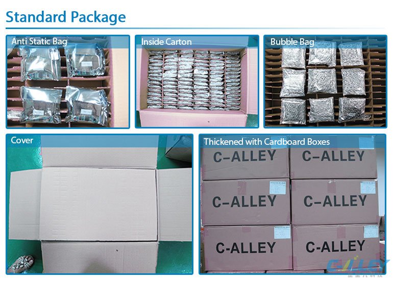
Standard Package
Each PCBA unit will be in Anti static bag, then the bubble bags, and then put into PCBA special carton

Please send Email to kspcba@c-alley.com or call us through +86 13828766801 Or submit your inquiry by online form. Please fill out below form and attach your manufacturing files( PCB Gerber files and BOM List) if need quotation. We will contact you shortly.
 +86 13828766801
 kspcba@c-alley.com
 https://www.kingshengpcba.com/
 2/F, Building 6, Tangtou 3rd Industrial Zone, Tangtou Community, Shiyan Town, Baoan District, Shenzhen, China, 518108