* On your first PCB Assembly order!
* Up to $300 discount

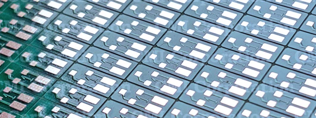
Kingsheng's panelized PCB and PCBA assembly service is a process of assembling multiple smaller boards onto a larger panel, which can be separated into individual boards after assembly. This process is commonly used in the electronics manufacturing industry to increase efficiency and reduce costs.
Panelization involves designing a larger panel that contains multiple smaller PCBs or PCBA units, with each unit being separated by V-Scored or stamp hole. The smaller units are then assembled onto the panel and tested as a whole before they are separated.
Panelized assembly allows for multiple smaller boards to be assembled at once, reducing the number of assembly steps and increasing production efficiency
Panelization reduces the cost of producing PCBs as it eliminates the need to set up individual PCBs on a production line. Instead, a single panel containing multiple PCBs can be processed at once, reducing setup times and labor costs.
Panelized assemblies are easier to handle during the assembly process, reducing the risk of damage to the individual boards.
Panelized PCBs undergo rigorous testing procedures before they are separated into individual boards. This ensures that each PCB meets strict quality standards, resulting in fewer defects and improved overall product reliability.
Kingsheng offers customized panelization services that allow customers to get the exact PCB size and configuration they need. This helps to reduce material waste and lowers production costs while ensuring the desired functionality of the final product.
Panelization allows multiple PCBs to be manufactured at the same time, significantly increasing production efficiency. This means that Kingsheng can produce more PCBs in less time, which is important for meeting tight deadlines and keeping up with customer demands.
The first step is to design the individual PCBs that need to be assembled. Ensure that they are designed with similar dimensions, layer stack-up, and components placement.
After designing the individual PCBs, create a panelization layout. This layout determines how the PCBs will be arranged on the panel. Pay attention to factors such as clearance, keep out zones, and fiducial markers positioning.
Once the panel is ready, components can be placed onto each PCB using automated pick and place machines. Solder paste is applied to the pads, and then the components are placed into position using the panel mounting pins as a guide.
Once the panel is ready, components can be placed onto each PCB using automated pick and place machines. Solder paste is applied to the pads, and then the components are placed into position using the panel mounting pins as a guide.
After the components have been placed, the panel is transferred to the reflow oven for soldering. Once complete, the panel undergoes an inspection process to ensure the quality of the assembly.
Finally, the individual PCBs are separated from the panel by breaking off the tabs or cutting along the routing lines.
Panelizing PCB&PCBA involves designing the individual PCBs, creating a panelization layout, adding tooling holes and routing, assembling the PCBs, reflow and inspection, and finally separating the individual PCBs from the panel.