* On your first PCB Assembly order!
* Up to $300 discount

Product Name Home Security PCB Assembly
1.PCBA Turnkey solution
2.PCB Assembly, PCB/PCBA Design, PCBA Copy
3.SMT&DIP&PTH&BGA Assembly
4.Component sourcing and purchasing
5.Quick prototyping
6.Test:X-Ray,AOI,In-Circuit Test(ICT),Functional Test(FCT)
7.High mix and low/medium volume are acceptable
What is a security PCB?
A specialized circuit board used for security and surveillance systems is called a security PCB (Printed Circuit Board). A wide range of security and surveillance devices, including as sensors, cameras, access control systems, alarm systems, smart doorbells, and more, are supported by these PCBs. In order to ensure the efficient operation of security and surveillance systems, security PCBs are designed with functionality and security, dependability, and performance in mind.
The process of creating, assembling, and manufacturing printed circuit boards (PCBs) specifically intended for smart devices is known as "smart home assembly." A smart home is a place of living that makes use of IOT, or internet-connected appliances, to provide remote control and monitoring of appliances and systems including heating, lighting, and automated controls. Within a smart home system or environment, smart home PCBs enable the connectivity, automation, and operation of various home apps. The market for smart devices in residential applications and cutting-edge technologies is expanding quickly.
It takes a thorough understanding of electronics, PCB design software, and manufacturing procedures to build a PCB for a smart home alarm system. It is crucial to carefully analyze the system's needs and optimize the design in order to maximize performance, dependability, and manufactureability.
The particular PCBs utilized in a smart home alarm system will vary based on the functions and design of the device. A single PCB may be used by some systems to do all tasks, while many PCBs connected by a backplane may be used by others to increase the functionality of the smart home alarm system. The integration of smart home alarm systems with energy management and home automation systems, together with enhanced data security and privacy, is the primary trend in these systems.
In order to develop and manufacture smart home PCBs, one must pay close attention to all relevant factors, think creatively, and have a thorough awareness of the issues that smart home technologies and gadgets will face in the future. Miniaturization, rapidly advancing technology, AI integration, power efficiency, small PCB sizes, and seamless wireless connectivity are driving changes in the industry. This development in industry and smart home technologies opens the door to the development of small, energy-efficient, and Internet of Things-integrated systems and gadgets. Direct machine learning and artificial intelligence (AI) integration into printed circuit boards improves response times and accuracy, reduces reliance on external resources, and increases device intelligence. The success of smart home PCBs will depend on a complete strategy that incorporates user experience, sustainability, and technology developments.
Home Security PCB Assembly Manufacturing Service
PCB files, PCB technical requirements, BOM, Assembly or soldering technical requirements, to be offered by customer.
One Stop PCBA service: Production of PCB from 1-32 Layer, Assembly components/material purchase, SMT production, PCBA Testing, PCBA aging, PCBA Packaging, PCBA Delivery.
Home Security PCB Assembly Manufacturing Quality
1. CE-EMC, UL, FCC, SGS, ROHS, ISO9001:2008, ISO14001:2004, TS16949 Certified.
2. 8 Dustproof SMT Lines and DIP Lines.
3. ESD and dust proof working uniform implemented.
4. Operators are strictly trained, and approved for suitable working station.
5. PCBA Production Equipments:HITACHI Screen Printer,FUJI NXT-II & FUJI XPF-L Modules
Automatic Solder-Paste Printer,Reflow Oven,Wave Solder Machine,AI DIP Machine.
6. PCBA Testing Equipments:ORT Machine,Drop Test Machine,Temperature & Humidity Test Chamber, 3D CMM, ROHS Inspection Machine,AOI, X-RAY Inspection.
7. PCBA Testing Capability:AOI(Automatic Optic Inspection),ICT(In-Circuit Test),FCT(Functional Circuit Test),X-Ray for BGAs.
8. Component Package including
Component range:
* 01005,0201,0402,0603,0805,1206,1608,2125,3216
* Fine Pitch QFP to 0.2mm
* BGA, Flip Chips, Connectors
* BGA to 0.2mm
9. SOP in every Work Station
10. PCB Materials: FR4, CEM-3, FPC, ALU
Home Security PCB Assembly Manufacturing Delivery Duration
Delivery for samples will be 10-15 WD after OEM Contact is signed and the Engineering Documents are confirmed.
For Mass production, based on the customer requirements, delivery can be done in several steps (Partial Delivery).
PCBA Manufacturing Additional Information
1. After the confirmation of Prototype, MP will be started.
2. DIP Components will be positioned only once, minimum distance between components and PCB Board will be maintained.
3. Positioning Holes and Grounding holes will be protected by high temperature resistance tape.
4. EPE Antistatic packaging is used to prevent shock and other problems.
Home Security PCB Assembly Shipment
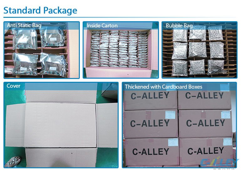
Standard Package
Each PCBA unit will be in Anti static bag, then the bubble bags, and then put into PCBA special carton

Please send Email to kspcba@c-alley.com or call us through +86 13828766801 Or submit your inquiry by online form. Please fill out below form and attach your manufacturing files( PCB Gerber files and BOM List) if need quotation. We will contact you shortly.
 +86 13828766801
 kspcba@c-alley.com
 https://www.kingshengpcba.com/
 2/F, Building 6, Tangtou 3rd Industrial Zone, Tangtou Community, Shiyan Town, Baoan District, Shenzhen, China, 518108