* On your first PCB Assembly order!
* Up to $300 discount
 C - A L L E Y
Home | Events | PCB | About Us | News | Contact Us
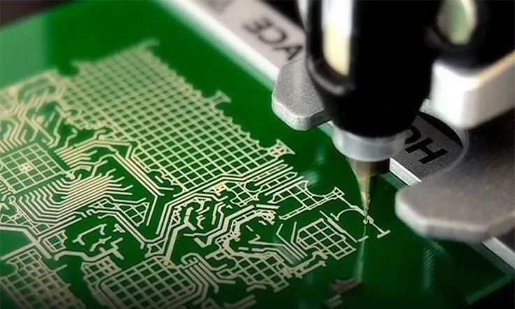
Currently, the typical process for printed circuit board (PCB) manufacturing employs a method known as "graphic plating." In this process, a layer of lead-tin corrosion-resistant coating is applied to the copper foil areas that will remain on the outer layer of the board—specifically, the parts that form the circuit design. The remaining copper foil is then removed through chemical means, a process referred to as etching.
At this stage, there are two layers of copper present on the board. During the outer etching process, it is necessary to completely etch away one layer of copper, leaving behind the required circuit on the other layer. The graphic plating method is characterized by having a copper layer that exists only beneath the lead-tin resist layer. Alternatively, there is a "full plate copper plating process," in which the entire plate is coated with copper, and only the area outside the sensitive film receives the lead-tin resist layer. One significant drawback of full plate copper plating is that the surface must undergo two plating processes, both of which will be corroded during etching. This can lead to various issues, especially when the wire width is very fine, and side corrosion can adversely affect the uniformity of the lines.
Another method used in the processing of the outer circuit of printed boards involves the use of a sensitive film instead of a metal coating as the corrosion-resistant layer. This approach is quite similar to the etching process for the inner layers.

Analysis of etching technology of PCB
Currently, tin or lead-tin is the most commonly used corrosion-resistant layer in the etching process, particularly with ammonia-based etching agents. Ammonia etching agents, which include ammonia water or ammonia chloride solutions, do not react with tin or lead-tin. Additionally, ammonia or ammonia sulfate etching solutions are available on the market.
Sulfate-based etching solutions allow for the separation of copper through electrolysis after use, enabling potential reuse. However, due to their low corrosion rate, these solutions are rarely utilized in actual production, although they are expected to find applications in chlorine-free etching. Some experiments have tested sulfuric acid-hydrogen peroxide as an etching agent for corroding outer patterns, but for various reasons—including economic factors and liquid waste treatment—this method has not seen widespread commercial adoption. Furthermore, sulfuric acid-hydrogen peroxide cannot be used with a lead-tin corrosion-resistant layer, making it an uncommon choice for producing outer layers of PCBs.
### 2. Etching Quality and Associated Problems
The fundamental requirement for etching quality is the complete removal of all copper layers except for those beneath the resist layer. In a more precise definition, etching quality also encompasses the consistency of wire width and the degree of side erosion. Due to the inherent properties of current etching solutions, etching occurs not only vertically but also horizontally, making side erosion almost unavoidable.
Side erosion is a significant etching parameter and is defined as the ratio of side erosion width to etching depth, referred to as the etching factor. In the printed circuit industry, this factor can vary considerably, ranging from 1:1 to 1:5. A lower degree of side etching or a low etching factor is generally preferred.
The design of the etching equipment and the specific composition of the etching fluid can influence the etching factor and the degree of side erosion, and these factors can ideally be controlled. Certain additives can help reduce side corrosion. However, the chemical composition of these additives is typically considered a trade secret, and manufacturers do not disclose this information publicly.
Why Choose China PCBA Supplier KSPCBA as Your Analysis of etching technology of PCB Manufacturer?
– Experienced and skilled team
– State-of-the-art equipment
– Strict quality control
– Excellent customer service
– Competitive price

Please send Email to kspcba@c-alley.com or call us through +86 13828766801 Or submit your inquiry by online form. Please fill out below form and attach your manufacturing files( PCB Gerber files and BOM List) if need quotation. We will contact you shortly.
 +86 13828766801
 kspcba@c-alley.com
 https://www.kingshengpcba.com/
 2/F, Building 6, Tangtou 3rd Industrial Zone, Tangtou Community, Shiyan Town, Baoan District, Shenzhen, China, 518108