* On your first PCB Assembly order!
* Up to $300 discount
 C - A L L E Y
Home | Events | PCBA | About Us | News | Contact Us
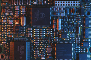
For PCB design, double or multi-panel is typically used, with each layer having a clear functional distinction. There are two types of packages in a multi-layer structure - pin package, where the via hole of the solder joint goes through the entire circuit board, and STM package, where the solder joint is restricted to the surface layer. The span is the distance between the terminals after the component is formed.

Circuit board PCB design and process
Here are the steps to prepare for PCB design:
1. Draw a schematic and generate a netlist. For simple circuit diagrams, you can design the PCB directly.
2. Enter the PCB design system and adjust the environmental parameters, like the size and type of grid points, cursor size and type, etc. You can use the system's default values.
3. Set the relevant parameters of the board, like the board's size and the number of layers.
4. Import the generated network table and check for errors in the circuit schematic design. Note that part packaging is essential when designing the PCB.
5. Arrange the position of each part package manually, even though the system has an automatic layout function.
6. Set the routing rules, including safety distance, wire form, etc. This is necessary for automatic routing.
7. Perform automatic routing using the system's complete function. Manual adjustment may be required for some lines.
8. Save the completed circuit diagram file and use various graphics output devices, like the printer or plotter output board, to create a wiring diagram.
Why Choose China PCBA Supplier KSPCBA as Your Circuit board PCB design and process Manufacturer?
– Experienced and skilled team
– State-of-the-art equipment
– Strict quality control
– Excellent customer service
– Competitive price

Please send Email to kspcba@c-alley.com or call us through +86 13828766801 Or submit your inquiry by online form. Please fill out below form and attach your manufacturing files( PCB Gerber files and BOM List) if need quotation. We will contact you shortly.
 +86 13828766801
 kspcba@c-alley.com
 https://www.kingshengpcba.com/
 2/F, Building 6, Tangtou 3rd Industrial Zone, Tangtou Community, Shiyan Town, Baoan District, Shenzhen, China, 518108