* On your first PCB Assembly order!
* Up to $300 discount
 C - A L L E Y
 Home | Events | PCB | About Us | News | Contact Us
PCB splicing is primarily done for production convenience. In a plate factory, the base material is typically large, allowing for multiple boards to be manufactured simultaneously and then cut individually. If splicing is mainly utilized for welding production, consider the scenario where a large nail cover board is welded one by one on an SMT machine as large as a car.
Definitions of PCB Panels
A PCB panel can be defined in several ways. "Convenience plug-in" refers to a method that both manufacturers and customers find beneficial, as it provides a way to save materials while meeting customer specifications. Manufacturers often implement convenience methods, such as V-cutting, to optimize material usage and minimize waste.
To enhance production efficiency and reduce costs during PCBA processing, circuit boards are typically assembled for production. This approach facilitates the patch welding process at PCBA manufacturing facilities. Below are some common methods and principles of PCBA circuit board assembly:
Principles of PCBA Circuit Board Assembly:
1. The width of the PCB panel should be ≤ 260mm (for SIEMENS lines) or ≤ 300mm (for FUJI lines). If automatic dispensing is needed, the size must be within 125mm × 180mm.
2. The shape of the PCB panel should be as close to square as possible, ideally in sizes such as 2x2, 3x3, or 4x4 panels. Care should be taken to avoid creating "yin and yang" plates.
3. The outer frame (clamping edge) of the PCB panel should feature a closed-loop design to prevent deformation after being fixed in place.
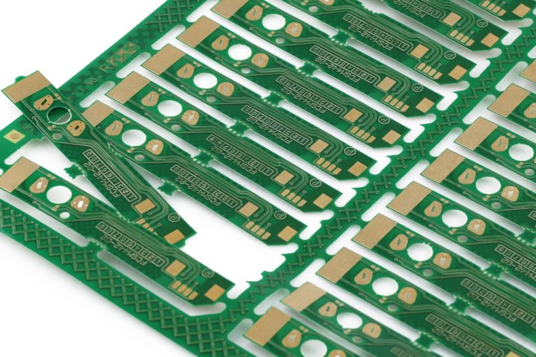
Common Splicing Methods of PCBA Circuit Board
4. The distance between small plates should be maintained between 75mm and 145mm.
5. Avoid placing large or protruding components near the connection points between the outer frame and the internal smaller boards, as well as between the smaller boards themselves. Leave a space greater than 0.5mm at the edges of the components and PCB to ensure the normal operation of the cutting tools.
6. Four positioning holes should be created at the four corners of the outer frame, with a hole diameter of 4mm ± 0.01mm. The strength of the holes must be adequate to prevent breakage during the plate handling process. Additionally, ensure high accuracy for the diameter and position, and that the hole walls are smooth and free from burrs.
7. Each small board within the PCB assembly must have a minimum of three positioning holes, with an aperture size ranging from 3mm to 6mm. No wiring or patches should be within 1mm of the edge positioning holes.
8. For QFPs with a spacing less than 0.65mm, reference marks for whole board positioning and fine pitch device positioning should be positioned at diagonal corners. Positioning datum symbols for sub-boards must be arranged in pairs at opposing corners of the positioning elements.
9. When establishing the datum locating point, it is advisable to reserve a non-blocking area that is 1.5mm larger than the locating point.
10. Large components should have positioning posts or holes, particularly for I/O interfaces, microphones, battery interfaces, microswitches, headphone interfaces, motors, etc.
Common Assembly Methods for PCBA Circuit Boards
1. V-Cut:
V-Cut refers to the process where multiple boards can be combined and spliced together. After PCB processing, a V-CUT machine creates a V-shaped slot between the boards, allowing for easy separation during use. This method is increasingly popular.
2. Flume:
The flume method involves milling grooves between circuit boards or within individual boards using a milling machine, essentially carving out the material as required.
3. Stamp Hole:
The stamp hole method links the plates using small holes that create a jagged, sawtooth appearance. This method requires precise burr control around the board, as only a few stamp holes can replace the V-Cut lines.
Why Choose China PCBA Supplier KSPCBA as Your PCBA Processing Manufacturer?
– Experienced and skilled team
– State-of-the-art equipment
– Strict quality control
– Excellent customer service
– Competitive price
Please send Email to kspcba@c-alley.com or call us through +86 13828766801 Or submit your inquiry by online form. Please fill out below form and attach your manufacturing files( PCB Gerber files and BOM List) if need quotation. We will contact you shortly.
 +86 13828766801
 kspcba@c-alley.com
 https://www.kingshengpcba.com/
 2/F, Building 6, Tangtou 3rd Industrial Zone, Tangtou Community, Shiyan Town, Baoan District, Shenzhen, China, 518108
We would also like to thank our customers for their trust and support. The company's outstanding achievements are mainly due to the loyalty of our customers, which also encourages and spurs our company to forge ahead.