* On your first PCB Assembly order!
* Up to $300 discount
 C - A L L E Y
 Home | Events | PCB | About Us | News | Contact Us
An essential aspect of PCBA (Printed Circuit Board Assembly) design is the SMT (Surface Mount Technology) pad. The pad's design determines the positioning of components on the PCBA and directly impacts the reliability of solder joints, the occurrence of welding defects, clarity during processing, and the ease of testing and maintenance. Therefore, effective pad design is crucial for the manufacturability of the entire PCBA.
For SMT chip components, pad design becomes even more critical. During the design phase, considerations must be made regarding whether the amount of solder will ensure reliable joints and whether there is a risk of undesirable issues such as bridging and warping during the reflow process. The compatibility between SMC (Surface Mount Component) / SMD (Surface Mount Device) and the pads must also meet specific requirements.
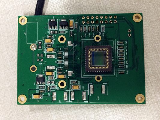
Dimensions of PCBA pads and design defects of chip components
Common defects in PCBA pad size design include size errors, incorrect spacing, and asymmetry. These issues can lead to problems such as false soldering, component displacement, insufficient solder, and poor tin availability during the SMT processing, ultimately affecting the board's reliability.
Defects in the design of SMT chip component pads can manifest in various ways:
1. The QFP (Quad Flat Package) pad being too long can result in short circuits.
2. A PLCC (Plastic Leaded Chip Carrier) socket pad that is too short may cause faulty soldering.
3. An excessively long pad for an IC (Integrated Circuit) can lead to excess solder, resulting in short circuits during reflow.
4. An overly long wing chip pad can hinder proper solder filling, leading to poor wettability at the heel.
5. Chip component pads that are either too short or improperly sized can result in displacement, open circuits, and difficulties in soldering, negatively impacting processing.
6. Poor pad design can affect the shape of solder joints and reduce their reliability.
7. Pads connected directly to large areas of copper foil can also lead to issues such as insufficient solder and faulty joints.
Shenzhen's established electronic processing factory offers high-quality SMT chip and PCBA processing services, providing a comprehensive one-stop electronic processing solution.
Why Choose China PCBA Supplier KSPCBA as Your PCBA pads and design Manufacturer?
– Experienced and skilled team
– State-of-the-art equipment
– Strict quality control
– Excellent customer service
– Competitive price
Please send Email to kspcba@c-alley.com or call us through +86 13828766801 Or submit your inquiry by online form. Please fill out below form and attach your manufacturing files( PCB Gerber files and BOM List) if need quotation. We will contact you shortly.
 +86 13828766801
 kspcba@c-alley.com
 https://www.kingshengpcba.com/
 2/F, Building 6, Tangtou 3rd Industrial Zone, Tangtou Community, Shiyan Town, Baoan District, Shenzhen, China, 518108
We would also like to thank our customers for their trust and support. The company's outstanding achievements are mainly due to the loyalty of our customers, which also encourages and spurs our company to forge ahead.