* On your first PCB Assembly order!
* Up to $300 discount
 C - A L L E Y
Home | Events | PCB | About Us | News | Contact Us
Printed Circuit Boards (PCBs) are designed to provide support and connections between electronic components. The board itself is made from non-conductive material to isolate each component from the others, and it only connects those components that are meant to be part of the board through conductive traces of copper. PCBs serve as the foundation of almost all electronic devices. This guide covers all the basic aspects of PCB manufacturing, including design, the manufacturing process, cost, equipment, and more.
What is PCB Manufacturing?
PCB manufacturing is a systematically complicated process that includes designing, testing, assembly, and inspection. The PCB manufacturing process begins with schematic design, after which the manufacturers turn the virtual PCB board design into a physical PCB board. Typically, PCB manufacturing involves mass production of standard PCBs. However, custom PCB manufacturing still holds a strong position in the electronic industry, as specialized boards can meet different electrical and mechanical requirements.
Different Types of PCB
1. Single Sided PCB or Single Layer PCB
2. Double Sided PCB or Double Layer PCB
3. Multilayer PCB
4. Rigid PCB
5. Flex PCB or Flexible PCB
6. Rigid-Flex PCB or Rigid-Flexible PCB
7. PCB Substrate and Core Materials

Electronics PCB Manufacturing
PCB Manufacturing Process Flowchart – Step by Step
Step-1: Patterning or Etching
Most printed circuit boards are manufactured by applying a layer of copper over the entire surface of the PCB substrate material either on one side or both sides. This creates a blank printed circuit board, with copper everywhere on the surface. From here the unwanted copper is removed by subtractive methods.
Step-2: Photoengraving
The photo engraving process uses a mask or photomask combined with chemical etching to subtract or remove the copper areas from the circuit board substrate. The photomask is created with a photoplotter which takes the design from CAD PCB software. Lower-resolution photomasks are sometimes created with the use of a laser printer using transparency.
Step-3: Lamination
Many printed circuit boards are made up of multiple layers; these are referred to as multi-layer printed circuit boards. They consist of several thin etched boards or trace layers and are bonded together through the process of lamination.
Step-4: Drilling
Each layer of the printed circuit board requires the ability of one layer to connect to another, this is done through drilling small holes called “VIAS“. These drilled holes require precision placement and are most commonly done with the use of an automated drilling machine. These machines are driven by computer programs and files called numerically controlled drill or NCD files also referred to as excellon files. These files determine the position and size of each drill in the design.
Step-5: Solder Plating (Solder Resist)
Pads and lands that will require electronic components to be mounted are plated to allow the solderability of the components. Bare copper is not readily solderable and requires the surface to be plated with a material that facilitates soldering. In the past, a lead-based tin was used to plate the surfaces, but with RoHS (Restriction of Hazardous Substances) compliance enacted newer materials are being used such as nickel and gold to both offer solderability and comply with RoHS standards.
Step-6: Silk Screen
When visible information needs to be applied to the board such as company logos, part numbers or instructions, silk screening is used to apply the text to the outer surface of the circuit board. Where spacing allows, screened text can indicate component designators, switch setting requirements and additional features to assist in the PCB assembly process.
Step-7: Testing
Unassembled circuit boards are subjected to a bare board test where each circuit connection is verified as correct on the finished circuit board. In high-volume circuit board production, a bed of nail tester or fixture is used to make contact with the copper lands or holes on one or both sides of the board to facilitate testing. Computers are used to control the electrical testing unit to send a small current through each contact point on the bed of nails and verify that such current can be detected on the appropriate contact points.
PCB Manufacturing Equipment
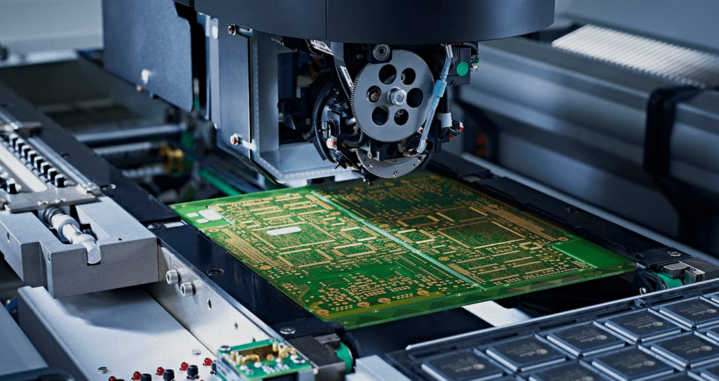
PCB manufacturing is a complex process that involves several steps, from base material cutting to final testing. Some of the essential equipment used in PCB manufacturing includes:
- Drilling machine (mechanical and laser)
- Etching equipment (chemical and plasma)
- Plating machine (electroless, electroplating)
- Exposure and developing equipment
- Automated optical inspection (AOI) equipment
- E-testing machine
- Flying probe tester
- Solder paste printing machine
- Automatic pick and place machine
- Reflow soldering oven
- Various testing equipment
After reading this, you should have a basic understanding of PCB manufacturing, including the processes involved, costs, and the equipment used. However, it's advisable to visit professional PCB manufacturing companies for a more in-depth understanding.
Why Choose China PCBA Supplier KSPCBA as Your Electronics PCB Manufacturing Manufacturer?
– Experienced and skilled team
– State-of-the-art equipment
– Strict quality control
– Excellent customer service
– Competitive price

Please send Email to kspcba@c-alley.com or call us through +86 13828766801 Or submit your inquiry by online form. Please fill out below form and attach your manufacturing files( PCB Gerber files and BOM List) if need quotation. We will contact you shortly.
 +86 13828766801
 kspcba@c-alley.com
 https://www.kingshengpcba.com/
 2/F, Building 6, Tangtou 3rd Industrial Zone, Tangtou Community, Shiyan Town, Baoan District, Shenzhen, China, 518108