* On your first PCB Assembly order!
* Up to $300 discount
 C - A L L E Y
Home | Events | PCB | About Us | News | Contact Us
1. Determining the board shape, size, and number of layers
When designing a printed circuit board, it's important to consider the shape and size of the product's structure. The board should be as simple as possible, typically a rectangle with a not too wide aspect ratio, to aid in assembly, improve production efficiency, and reduce labor costs.
The number of layers should be based on circuit performance, board size, and circuit density. Four-layer and six-layer boards are the most common choices. For example, a four-layer board has two conductor layers (component surface and soldering surface), a power layer, and a ground layer.
The layers of a multi-layer board should be symmetrical, ideally with an even number of copper layers, such as four, six, or eight. Asymmetrical lamination may cause board warping, especially for surface-mounted boards, so this should be carefully considered.
2. Component location and orientation
The placement of components should align with the circuit principles to ensure the board's performance. Particularly for high-frequency analog circuits, careful placement is crucial. An analysis of the circuit principle should guide the layout, with special attention given to the placement of key components. The overall structure of the printed board should also be considered to ensure an organized and convenient layout for assembly and maintenance.

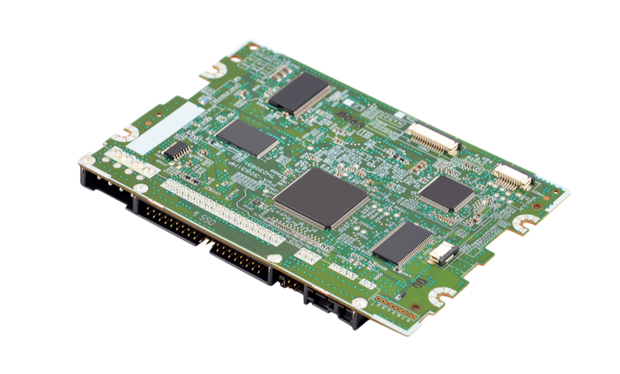
Essentials of multi-layer PCB design
3. Wiring layer and area requirements
Wiring should be based on circuit function. Outer layer wiring should have more wiring on the soldering surface and less on the component surface to aid in maintenance and troubleshooting. Thin, dense wires and sensitive signal wires are usually placed in the inner layer. The distribution of copper foil in the inner and outer layers should be even to reduce board warping and ensure uniformity during electroplating. A distance greater than 50 mils should be maintained between the conductive patterns of inner and outer layer wiring areas to prevent inter-layer short circuits during mechanical processing.
4. Wire direction and width requirements
Power, ground, and signal layers should be separated to minimize interference. Lines of adjacent layers should be as perpendicular as possible to reduce coupling and interference. Wire length should be minimized, especially for small signal circuits, to reduce resistance and interference. Signal lines on the same layer should avoid sharp corners when changing directions. The wire width should match the circuit's current and impedance requirements. Power input lines should be wider, while signal lines can be narrower. Consistency in line width is important for impedance matching.
Why Choose China PCBA Supplier KSPCBA as Your multi-layer PCB design Manufacturer?
– Experienced and skilled team
– State-of-the-art equipment
– Strict quality control
– Excellent customer service
– Competitive price

Please send Email to kspcba@c-alley.com or call us through +86 13828766801 Or submit your inquiry by online form. Please fill out below form and attach your manufacturing files( PCB Gerber files and BOM List) if need quotation. We will contact you shortly.
 +86 13828766801
 kspcba@c-alley.com
 https://www.kingshengpcba.com/
 2/F, Building 6, Tangtou 3rd Industrial Zone, Tangtou Community, Shiyan Town, Baoan District, Shenzhen, China, 518108