* On your first PCB Assembly order!
* Up to $300 discount
 C - A L L E Y
Home | Events | PCB | About Us | News | Contact Us
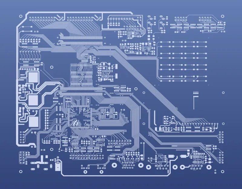
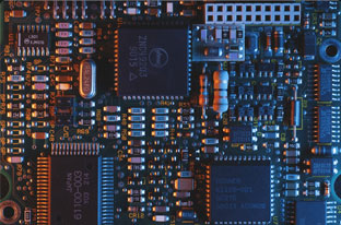
The importance of PCB boards in supporting electronic products and smart home appliances can't be overstated. They are crucial to meeting the requirements of most electronic products, making our terminal equipment more realistic. The fifteen steps of PCB board production are all important.
Step 1: PCB board design and output work
The design and output work involves the use of various design software and different versions of PCB design software. Differences can occur due to the use of different software which requires different GERBER files containing important coding information.
Step 2: PCB board printing film work
This step requires extremely high accuracy. Precise printing equipment is used to provide a detailed and accurate design of the film. Each layer of the circuit board has its own transparent and black film. The alignment of the film is crucial for a perfect connection.
Step 3: Inner layer
This step effectively produces PCB using a laminate to receive and form the ideal body of copper. The two sides of the copper must be glued in advance to ensure high cleanliness and prevent short circuits or open circuits.
Step 4: Copper etching
Solvents are used to remove unnecessary copper, and the hardened resist that protects the preferred copper needs to be washed off. The circuit board is left with only the required copper substrate for the PCB.
Step 5: Layer stacking
Optical tests are used to find inconsistencies. If necessary, professional technology personnel evaluate the process before the PCB can enter the final production stage.

Fifteen Steps For Making PCB Board
Step 6: Paste work
Applying paste to the PCB board is a delicate task that requires the expertise of a technician. The prepreg layer is first placed on the alignment groove, and then the paste is applied layer by layer using a bonding press.
Step 7: Drilling work and electroplating
Drilling the PCB board requires precision in selecting the drill bit size and skillful handling of the drilling process. Technicians control the computer-driven process until the drilling is completed. Any extra copper on the edge of the production panel is removed using analysis tools. Electroplating involves using chemical deposition to fuse the components.
Step 8: Outer layer imaging
This step must be carried out in a dust-free environment. UV lamps are used for photoresist etching to ensure proper alignment of the panel. Finally, the external panel is inspected to remove any unnecessary lithography from the previous stage.
Step 9: Repeat the electroplating work
Electroplating is a critical step that needs to be repeated and carefully checked in the PCB production process.
Step 10: Etching work
Etching work is essential to ensure the connectivity of conductive areas. Unwanted exposed copper and copper under the resist layer are removed, protecting valuable copper and ensuring its proper establishment and connection to the conductive area.
Step 11: Soldering and mask operation
Before applying the solder mask to both sides of the circuit board, the panel is cleaned and covered with epoxy solder ink. The circuit board is exposed to ultraviolet rays and then passed through the solder mask to the photographic film before entering the oven for the solder mask to cure.
Step 12: Surface treatment
To enhance the soldering capacity of the PCB, electroless plating with gold or silver is conducted. Some PCBs may also receive hot air flat pads at this stage, resulting in a surface finish.
Step 13: Screen printing
The nearly completed circuit board receives inkjet markings on its surface to indicate all important information related to the PCB. The PCB then enters the final coating and curing stage.
Step 14: Electrical testing
Electrical testing involves comparing the completed work with the initial design to ensure consistency.
Step 15: Cutting work
Different boards are cut from the original panel using routers or V-grooves. Routers leave small tabs along the edge of the board, while V-shaped grooves cut diagonal channels along both sides of the board.
Why Choose China PCBA Supplier KSPCBA as Your Making PCB Board Manufacturer?
– Experienced and skilled team
– State-of-the-art equipment
– Strict quality control
– Excellent customer service
– Competitive price

Please send Email to kspcba@c-alley.com or call us through +86 13828766801 Or submit your inquiry by online form. Please fill out below form and attach your manufacturing files( PCB Gerber files and BOM List) if need quotation. We will contact you shortly.
 +86 13828766801
 kspcba@c-alley.com
 https://www.kingshengpcba.com/
 2/F, Building 6, Tangtou 3rd Industrial Zone, Tangtou Community, Shiyan Town, Baoan District, Shenzhen, China, 518108