* On your first PCB Assembly order!
* Up to $300 discount
 C - A L L E Y
 Home | Events | PCB | About Us | News | Contact Us
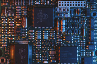
The systematic quality control of solder paste printing and reflow temperature management during SMT chip processing are crucial stages in the PCBA manufacturing process. For the production of high-precision circuit boards with special and complex designs, it is essential to utilize laser steel mesh under specific conditions. This ensures that the circuit boards meet higher quality and processing requirements. Depending on PCB manufacturing needs and customer product specifications, some circuit boards may require U-shaped holes or a reduction in the size of the steel mesh holes. The steel mesh must be processed according to the requirements of PCBA processing technology.
1. SMT Chip Assembly
Quality control in solder paste printing and reflow temperature management during SMT chip processing are critical factors in the PCBA manufacturing process. The use of laser steel mesh is necessary for printing high-precision circuit boards with specialized and intricate processes. This ensures that the boards meet the heightened quality and processing standards that are often necessary. Depending on the requirements of PCB manufacturing and specific customer characteristics, modifications such as the addition of U-shaped holes or alterations in steel mesh hole sizes may be essential. The steel mesh should be processed in alignment with PCBA processing technology standards.
The accuracy of temperature control in the reflow soldering furnace is vital for the effectiveness of solder paste and the quality of steel mesh soldering. Adjustments can be made according to the standard operating procedures (SOP). To minimize quality defects in the SMT segment of PCBA chip processing, strict adherence to automated optical inspection (AOI) testing can significantly reduce human error-related defects.

Four Problems in PCBA Chip Processing
2. DIP Plug-In Post-Welding
Post-soldering of DIP plug-in components is the final and one of the most important steps in PCB processing. During this phase, careful consideration must be given to the furnace pass fixtures used in wave soldering. Effectively utilizing these fixtures can enhance the qualification rate of products and minimize soldering issues such as excess solder, insufficient solder, and solder voids. To meet varying customer requirements, PCBA processing plants must continuously gather practical experiences and make technical advancements based on these insights.
3. Testing and Procedure Firing
Before commencing full-scale production, a manufacturability report should be generated following the receipt of the production contract from the customer. The initial design for manufacturability (DFM) report can provide valuable suggestions, such as identifying key test points on the PCB. This facilitates PCB soldering tests and subsequent evaluations of circuit continuity and connectivity following PCBA processing. Whenever feasible, it’s beneficial to communicate with the customer about backend programming and transfer the PCBA program to the core master IC using a burner. This approach allows for a more effective touch-based assessment of the complete PCBA and timely identification of defective products.
4. PCBA Manufacturing Test
Many customers seeking comprehensive PCBA processing services also require backend testing. This testing typically includes ICT (In-Circuit Testing), FCT (Functional Testing), burn tests (aging tests), temperature and humidity assessments, and drop tests.
Why Choose China PCBA Supplier KSPCBA as Your PCBA Chip Processing Manufacturer?
– Experienced and skilled team
– State-of-the-art equipment
– Strict quality control
– Excellent customer service
– Competitive price
Please send Email to kspcba@c-alley.com or call us through +86 13828766801 Or submit your inquiry by online form. Please fill out below form and attach your manufacturing files( PCB Gerber files and BOM List) if need quotation. We will contact you shortly.
 +86 13828766801
 kspcba@c-alley.com
 https://www.kingshengpcba.com/
 2/F, Building 6, Tangtou 3rd Industrial Zone, Tangtou Community, Shiyan Town, Baoan District, Shenzhen, China, 518108
We would also like to thank our customers for their trust and support. The company's outstanding achievements are mainly due to the loyalty of our customers, which also encourages and spurs our company to forge ahead.