* On your first PCB Assembly order!
* Up to $300 discount
 C - A L L E Y
Home | Events | PCBA | About Us | News | Contact Us
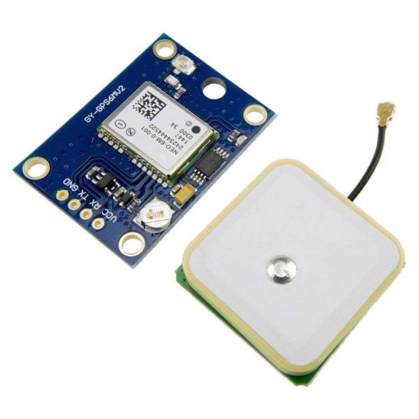
Nowadays, many devices use GPS for tracking and locating lost devices. When designing a GPS antenna PCB, it's crucial to follow specific rules and guidelines. You can find tutorials online to help with this process. Here are some important steps and techniques for successfully designing a GPS PCB.
1. Properly isolate or protect all components on the circuit board to prevent signal degradation from GPS antennas and receivers. If the receiver has a built-in antenna, receiver noise can cause issues, mainly due to insufficient shielding. The GPS signal must be extracted from the LNA by placing a SAW filter or a surface acoustic wave filter between the LNA and the receiver input.

GPS antenna PCB design and layout
2. Shielding, grounding, and wiring are essential for a GPS antenna PCB, as the GPS antenna cannot accept as much noise signal as other devices. To achieve this, create separate terrain for each block on the main PCB and add these terrain points to the star topology. Keep the antenna path away from the digital path, and if possible, route the antenna through the shielding cabinet to shield the antenna signal.
3. Attenuation and impedance matching are crucial in high-frequency PCB design. Longer traces and higher carrier frequencies can result in lower sensitivity, so it's important to select a shorter trace between the passive antenna and the external LNA for higher sensitivity. It's best to avoid vias in antenna traces to prevent increasing the impedance of the trace and potential inductive discontinuities.
After completing the PCB design, the design should be sent to a PCB manufacturer for manufacturing. Once the components are assembled, the PCB can be used.
The demand for antenna PCB design is increasing, and PCB designers need to understand and follow guiding principles to achieve a perfect antenna PCB layout. With the use of higher-quality software and advanced technology, such as artificial intelligence, designing antenna PCBs will become easier in the future.
Why Choose China PCBA Supplier KSPCBA as Your GPS antenna PCB design and layout Manufacturer?
– Experienced and skilled team
– State-of-the-art equipment
– Strict quality control
– Excellent customer service
– Competitive price

Please send Email to kspcba@c-alley.com or call us through +86 13828766801 Or submit your inquiry by online form. Please fill out below form and attach your manufacturing files( PCB Gerber files and BOM List) if need quotation. We will contact you shortly.
 +86 13828766801
 kspcba@c-alley.com
 https://www.kingshengpcba.com/
 2/F, Building 6, Tangtou 3rd Industrial Zone, Tangtou Community, Shiyan Town, Baoan District, Shenzhen, China, 518108