* On your first PCB Assembly order!
* Up to $300 discount
 C - A L L E Y
Home | Events | PCB | About Us | News | Contact Us
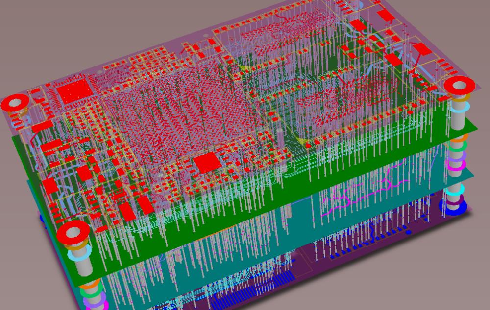
Before designing a multi-layer PCB circuit board, PCB layout engineers must determine the board's structure based on the circuit scale, board size, and electromagnetic compatibility (EMC) requirements. This will involve deciding whether to use a 4-layer, 6-layer, or a circuit board with even more layers. Below are the design steps and precautions for multi-layer PCB boards.
Steps for Multi-layer PCB Design
The design process for multi-layer PCB circuit boards is fundamentally similar to that of ordinary PCB boards and can be broken down into the following steps:
1. Planning the Circuit Board: This step focuses on defining the physical dimensions of the PCB, the packaging format of the components, the installation methods for the components, and the layer structure—whether it is a single-layer, double-layer, or multi-layer board.
2. Setting Working Parameters: This involves configuring the working environment and the parameters for each layer. Proper and reasonable setting of the PCB environmental parameters can greatly enhance design convenience and improve efficiency.
3. Component Layout and Adjustment: Once the initial preparations are complete, the netlist can be imported into the PCB design software. Component layout and adjustment are crucial tasks in PCB design, as they directly influence subsequent routing and the configuration of internal electrical layers.

Introductory Tutorial for Multilayer PCB Design
4. Defining the Middle Layer Structure: This step focuses on establishing the specific layer structure in the layer stack manager of the design software. It involves determining the number of intermediate signal layers and internal electrical layers, as well as the configurations of the upper and lower layers.
5. Segmenting Internal Electrical Layers: In multi-layer boards, internal electrical layers often contain multiple power networks. It's necessary to divide these layers into isolated areas, with each connected to specific power networks. This step is critical, as it significantly impacts the routing of power and ground grids, as well as the overall layout and routing of components.
6. Setting Wiring Rules: This involves specifying all aspects of circuit wiring, including wire width, spacing between parallel lines, safety distances between wires and pads, and via sizes. Regardless of the wiring method employed, establishing wiring rules is essential to ensure safety, meet manufacturing requirements, and reduce costs.
7. Wiring and Adjustment: While the system typically offers automatic wiring features, they often fail to meet the designer's specifications. In practice, designers frequently rely on manual wiring or a combination of partially automatic and manual wiring to complete this task. It is crucial to pay attention to the layout and wiring and to the characteristics of the PCB's internal electrical layers, as the layout may need to be adjusted based on wiring needs or vice versa.
8. Other Auxiliary Operations: This includes processes like copper plating and teardrop repairs, as well as documentation tasks such as output reporting and printing. These documents serve to check and modify PCB circuit boards, as well as to create a list of components for purchasing.
By following these steps and considerations, engineers can effectively design a multi-layer PCB that meets the specified requirements.
Why Choose China PCBA Supplier KSPCBA as Your Introductory Tutorial for Multilayer PCB Design Manufacturer?
– Experienced and skilled team
– State-of-the-art equipment
– Strict quality control
– Excellent customer service
– Competitive price

Please send Email to kspcba@c-alley.com or call us through +86 13828766801 Or submit your inquiry by online form. Please fill out below form and attach your manufacturing files( PCB Gerber files and BOM List) if need quotation. We will contact you shortly.
 +86 13828766801
 kspcba@c-alley.com
 https://www.kingshengpcba.com/
 2/F, Building 6, Tangtou 3rd Industrial Zone, Tangtou Community, Shiyan Town, Baoan District, Shenzhen, China, 518108