* On your first PCB Assembly order!
* Up to $300 discount
 C - A L L E Y
Home | Events | PCB | About Us | News | Contact Us
Selection and Stacking Principles of Multilayer PCB Layers
Determining the stacked structure of a multilayer PCB involves various factors. From a wiring perspective, having more layers generally improves the routing capability. However, this increase comes with higher costs and greater manufacturing complexity. Manufacturers often prioritize whether the stacked structure is symmetrical, so selecting the number of layers requires a careful balance of multiple considerations to achieve optimal results.
Experienced designers typically analyze the wiring constraints after completing the initial layout of components. By utilizing EDA tools, they assess the wiring density of the circuit board. They then evaluate the number and types of signal lines that have special wiring requirements, such as differential pairs and sensitive signals, to establish how many signal layers are needed. Following this, they determine the number of inner electrical layers based on power supply types, isolation needs, and interference mitigation requirements. This process essentially defines the total number of layers for the circuit board.
After establishing the layer count, the next step is to arrange the components on each layer efficiently. This arrangement should consider two main factors:
1. Distribution of special signal layers.
2. Distribution of the power supply and ground layers.

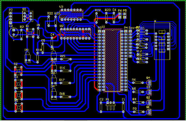
Multi-layer PCB Stack Structure
General Principles of Component Layout
Designers should adhere to the following general principles during the PCB layout process:
1. Prefer Single-Sided Component Placement: It is advisable to place all components on one side of the board. If components must be placed on both sides, pin-type components should ideally be on the bottom layer to facilitate better placement and soldering. SMD components are more suitable for the bottom layer, similar to the layout on common computer graphics card PCBs. Arranging components on a single side simplifies silk-screening and reduces costs.
2. Strategically Position Interface Components: Connectors, which link the circuit board to external sources (like power and signal lines), should generally be located along the board's edge (e.g., serial and parallel ports). Central placement may hinder wiring and connectivity due to component density. Additionally, ensure the interface components are oriented to allow smooth wire exits from the board. After placement, clearly label the type of interface, including voltage levels for power interfaces, to prevent connection errors that could damage the board.
3. Maintain Electrical Isolation Zones: A sufficient gap should exist between high-voltage and low-voltage components. Keeping components with significantly different voltage levels apart not only enhances electrical insulation but also aids in signal isolation and interference reduction.
4. Group Closely Connected Components: Place components that are electrically related in proximity, following the modular approach for layout.
5. Minimize Noise Disturbances:** Components prone to generating noise, such as clock generators and crystal oscillators, should be placed as near as possible to the CPU's clock input. Furthermore, high-current and switching circuits can also generate noise. As a best practice, keep these components away from high-speed signal circuits, like logic control and storage circuits. Whenever feasible, consider integrating the control board with the power board to enhance the circuit board's anti-interference capability and overall reliability.
Why Choose China PCBA Supplier KSPCBA as Your Multi-layer PCB Manufacturer?
– Experienced and skilled team
– State-of-the-art equipment
– Strict quality control
– Excellent customer service
– Competitive price

Please send Email to kspcba@c-alley.com or call us through +86 13828766801 Or submit your inquiry by online form. Please fill out below form and attach your manufacturing files( PCB Gerber files and BOM List) if need quotation. We will contact you shortly.
 +86 13828766801
 kspcba@c-alley.com
 https://www.kingshengpcba.com/
 2/F, Building 6, Tangtou 3rd Industrial Zone, Tangtou Community, Shiyan Town, Baoan District, Shenzhen, China, 518108