* On your first PCB Assembly order!
* Up to $300 discount
 C - A L L E Y
Home | Events | PCB | About Us | News | Contact Us
As a newcomer in the realm of switching power supplies, LED switching power supplies have found widespread applications in various fields. During the development of new products, the layout of components on the PCB (Printed Circuit Board) plays a crucial role in designing LED switching power supplies. This aspect is also a key factor in evaluating an engineer's design scheme. So, what steps can be taken to achieve optimal results in the layout of PCB components?
First and foremost, it's essential to carefully consider the size of the PCB. If the PCB size is excessively large, the longer printed lines can lead to increased impedance, reduced noise immunity, and higher costs. Conversely, if the PCB is too small, it may not dissipate heat effectively, and adjacent lines may be more prone to interference. Typically, the ideal shape for a PCB circuit board in LED switching power supplies is rectangular, with an aspect ratio of either 3:2 or 4:3. It's also important that components located at the edge of the circuit board are positioned at least 2mm away from the edge.

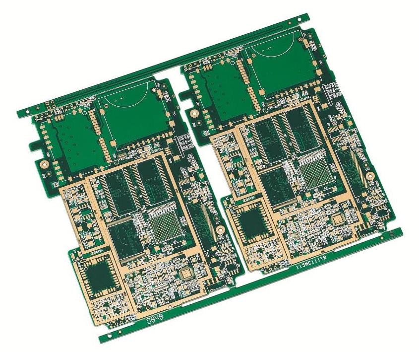
Optimal layout of LED switching power supply with PCB components
Secondly, once the PCB size is finalized, attention must turn to the distribution of components, especially for circuits operating under high-frequency conditions. Components should be arranged in parallel as much as possible, which enhances aesthetics, simplifies installation and soldering, and facilitates mass production.
When placing the components on the PCB, it’s crucial not to focus solely on speed. Future soldering challenges must be considered, prompting engineers to ensure a reasonable layout and avoid overcrowding between components. Emphasis should be placed on the core components of each functional circuit, arranging the overall component layout around these key parts. It’s essential for components to be evenly, neatly, and compactly arranged on the PCB, minimizing and shortening the leads and connections between components. Additionally, decoupling capacitors should be positioned as close as possible to the VCC of the device.
Finally, when arranging the PCB components for the LED switching power supply, engineers should organize each functional circuit unit according to the circuit process. Such a layout will facilitate more effective and faster signal flow, keeping the signal flowing in the same direction as much as possible. During the layout process, the primary objective should be to ensure consistent distribution of wiring, paying careful attention to the connection of flying leads when relocating devices, and clustering connected components together. The loop area should be minimized to suppress any radiation interference from the switching power supply.
By following these guidelines, the LED switching power supply can achieve an optimal PCB component layout.
Why Choose China PCBA Supplier KSPCBA as Your Optimal layout of LED switching power supply with PCB components Manufacturer?
– Experienced and skilled team
– State-of-the-art equipment
– Strict quality control
– Excellent customer service
– Competitive price

Please send Email to kspcba@c-alley.com or call us through +86 13828766801 Or submit your inquiry by online form. Please fill out below form and attach your manufacturing files( PCB Gerber files and BOM List) if need quotation. We will contact you shortly.
 +86 13828766801
 kspcba@c-alley.com
 https://www.kingshengpcba.com/
 2/F, Building 6, Tangtou 3rd Industrial Zone, Tangtou Community, Shiyan Town, Baoan District, Shenzhen, China, 518108