* On your first PCB Assembly order!
* Up to $300 discount
 C - A L L E Y
 Home | Events | PCB | About Us | News | Contact Us
Understanding Packaging Defects and Failures in PCBA Processing
Electronic devices are highly complex systems, and the defects and failures that occur during the packaging process are equally intricate. Therefore, studying these defects and failures requires a systematic understanding of the packaging process, allowing for a multi-faceted analysis of their causes.
Research Methodology for Packaging Defects and Failures
The failure mechanisms in packaging can be categorized into two types: overstress and wear.
- Overstress failure typically occurs suddenly and can be catastrophic.
- Wear failure, on the other hand, involves long-term cumulative damage, initially manifesting as performance degradation before ultimately leading to device failure.
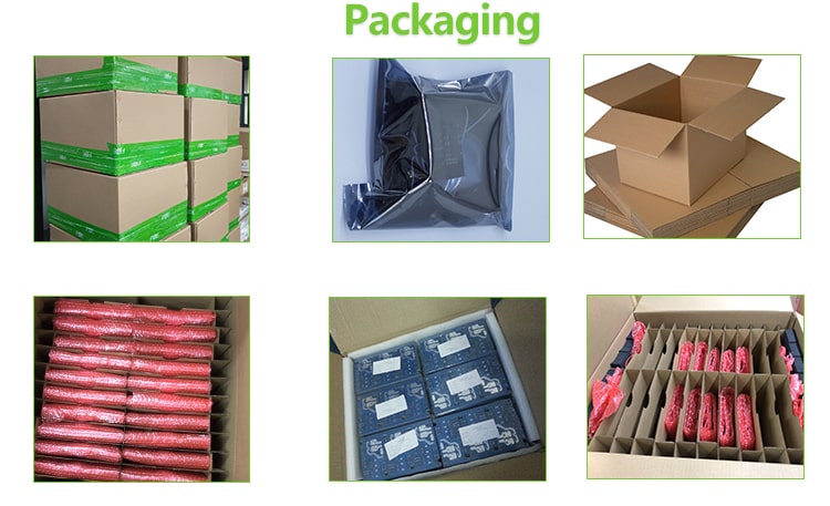
Packaging in PCBA Processing
The types of failure loads include mechanical, thermal, electrical, radiation, and chemical loads.
Numerous factors can influence packaging defects and failures, such as material composition and properties, packaging design, environmental conditions, and process parameters. Identifying these influencing factors is crucial for preventing defects and failures.
These factors can be determined through experimentation or simulation, often employing methods such as physical modeling and numerical parameter analysis. In cases involving more complex defects and failure mechanisms, the trial-and-error method may be used to pinpoint key influencing factors, though this approach tends to require more extended testing periods and equipment adjustments, making it less efficient and more costly.
Types of Loads Causing Failure
The loads that can lead to packaging failures are categorized into:
- Mechanical Loads
- Thermal Loads
- Electrical Loads
- Radiation Loads
- Chemical Loads
Classification of Packaging Defects
Common packaging defects include:
- Lead deformation
- Base offset
- Warpage
- Chip breakage
- Delamination
- Voids
- Uneven packaging
- Burrs
- Foreign particles
- Incomplete curing
This overview highlights the causes and manifestations of packaging defects and failures in PCBA processing, as explained by circuit board design and manufacturer practices.
Why Choose China PCBA Supplier KSPCBA as Your Packaging in PCBA Processing Manufacturer?
– Experienced and skilled team
– State-of-the-art equipment
– Strict quality control
– Excellent customer service
– Competitive price
Please send Email to kspcba@c-alley.com or call us through +86 13828766801 Or submit your inquiry by online form. Please fill out below form and attach your manufacturing files( PCB Gerber files and BOM List) if need quotation. We will contact you shortly.
 +86 13828766801
 kspcba@c-alley.com
 https://www.kingshengpcba.com/
 2/F, Building 6, Tangtou 3rd Industrial Zone, Tangtou Community, Shiyan Town, Baoan District, Shenzhen, China, 518108
We would also like to thank our customers for their trust and support. The company's outstanding achievements are mainly due to the loyalty of our customers, which also encourages and spurs our company to forge ahead.