* On your first PCB Assembly order!
* Up to $300 discount
 C - A L L E Y
Home | Events | PCB | About Us | News | Contact Us
In the PCB manufacturing process, welding is a crucial step. It not only involves fixing components onto the PCB board but also requires that the solder joints are firm and smooth. The quality of welding directly impacts the success of PCB production; therefore, mastering welding techniques is essential for every PCB manufacturer. Here are the key points of welding:
1. Welding Method
Components must be clean and tinned. Electronic components exposed to air can develop an oxide layer on their pins due to oxidation, along with other contaminants. Before welding, it's necessary to scrape off the oxide layer using a knife and immediately apply a layer of solder (commonly called tin) before proceeding with welding. This preparation makes the component easier to weld and minimizes the risk of cold solder joints.
2. Welding Temperature and Time
When welding, the temperature of the soldering iron should be higher than that of the solder, but not excessively so, as this can cause the rosin to smoke. If the welding time is too short, the solder joint may not reach a sufficient temperature to melt adequately, resulting in rough solder joints and a higher chance of cold solder issues. Conversely, if the welding time is too long, the solder may flow excessively, which can overheat and damage the components.
3. Positioning of the Soldering Iron and Welding Points
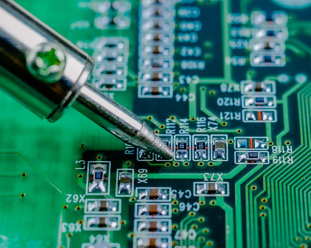
The soldering tip should make contact with the welding point's surface to maximize the heat transfer area, allowing for faster welding.

PCB Circuit Board Welding Technology
4. Post-Welding Inspection
After welding, it's vital to check for missed solder joints, cold solder joints, and potential short circuits caused by solder overflow. These issues can be subtle; using tweezers to gently pull the component pins can help identify weak connections. If any movement is detected, immediate repairs should be made.
Weldability of PCB Circuit Boards
PCB circuit boards serve as the support structure for electronic components and provide electrical connections between them. They can be categorized based on the number of circuit layers into single-sided, double-sided, and multi-layer boards. Common multi-layer boards typically have four or six layers, while complex designs can exceed ten layers.
To ensure the printed board has a long shelf life and maintains a good wetting effect for solder, solderability treatment must be applied to the surface. Solderability refers to how well a metal surface can be wetted by molten solder. This is a significant consideration, as proper solderability treatment is crucial for maintaining the PCB's functionality over time.
Being essential in various power supply products, PCBs are prevalent in everyday life. Therefore, it is imperative that manufacturers prioritize quality during production, address any potential product failures promptly, and mitigate economic losses.
Why Choose China PCBA Supplier KSPCBA as Your PCB Circuit Board Welding Technology Manufacturer?
– Experienced and skilled team
– State-of-the-art equipment
– Strict quality control
– Excellent customer service
– Competitive price

Please send Email to kspcba@c-alley.com or call us through +86 13828766801 Or submit your inquiry by online form. Please fill out below form and attach your manufacturing files( PCB Gerber files and BOM List) if need quotation. We will contact you shortly.
 +86 13828766801
 kspcba@c-alley.com
 https://www.kingshengpcba.com/
 2/F, Building 6, Tangtou 3rd Industrial Zone, Tangtou Community, Shiyan Town, Baoan District, Shenzhen, China, 518108