* On your first PCB Assembly order!
* Up to $300 discount
 C - A L L E Y
 Home | Events | PCB | About Us | News | Contact Us
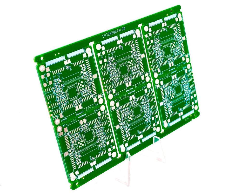
The process of copying a printed circuit board (PCB) involves several straightforward steps. First, you scan the PCB that needs to be copied and record the precise positions of the components. After that, disassemble the components to create a bill of materials (BOM) and arrange for material procurement. Next, scan a blank PCB and process the image with PCB copying software to create a PCB drawing file. Finally, send the PCB file to a manufacturing factory for production. Once the board is made, solder the purchased components onto the newly created PCB. At this point, you can proceed to test and debug the circuit board.
Specific Steps for PCB Copying
1. Document the PCB: Obtain the PCB and record the models, parameters, and positions of all components on paper. Pay particular attention to the directions of diodes, transistors, and IC notches. It is advisable to take two photos of the positions of the major components using a digital camera, as PCBs are becoming increasingly complex and some components may not be easily visible.
2. Prepare the PCB for Scanning: Remove all components from the multilayer board and eliminate any solder from the pad holes. Clean the PCB with alcohol, then place it in a scanner. When scanning, increase the pixel resolution to obtain a clearer image. Lightly polish the top and bottom layers with fine-grit sandpaper until the copper film shines. Place the polished board into the scanner and use PHOTOSHOP to scan both layers in color. Ensure that the PCB is scanned horizontally and vertically, as incorrect alignment will render the scanned images unusable.
3. Adjust the Scanned Image: Modify the contrast and brightness of the image to create a strong distinction between the copper film and the blank areas. Convert the secondary image to black and white to check for clarity in the lines. If the lines are unclear, repeat this step. Once satisfied, save the images as black and white BMP files named TOP.BMP and BOT.BMP. Any graphics issues can be repaired and corrected using PHOTOSHOP.
PCB Copying Technology of Electronic Manufacturers
4. Convert BMP Files to PROTEL Files: Import the two BMP files into PROTEL. Ensure that the positions of the pads and vias on the two layers align correctly, indicating successful previous steps. If there is any misalignment, repeat step three. It’s important to take your time with this process, as even a minor issue can impact the quality of the copied PCB.
5. Create the PCB Layers: Convert the BMP file of the top layer to a TOP PCB file. Be sure to convert it to the SILK layer (the yellow layer). Trace the lines on the TOP layer and place components according to the layout established in Step 2. Once done, delete the SILK layer and repeat this process until all layers have been drawn.
6. Combine the Layers: In PROTEL, load the TOP. PCB and BOT. PCB files, then combine them into a single image file.
7. Print and Compare: Use a laser printer to print the TOP and BOTTOM layers on a transparent film at a 1:1 ratio. Overlay the film onto the PCB and verify that there are no errors. If everything is correct, you have successfully created a copy of the original board. However, this is only half of the process; you must also test whether the electronic performance of the copied board matches that of the original. If the performance is identical, the process is complete.
Note: If working with a multilayer board, carefully polish it down to the inner layer and repeat steps three to five simultaneously for each layer. The naming convention for the files should reflect the number of layers. Generally, copying double-sided boards is simpler than copying multilayer boards, which are more prone to misalignment. Therefore, special care should be taken with multilayer boards to avoid issues with internal and external vias.
Why Choose China PCBA Supplier KSPCBA as Your PCB Copying Technology Manufacturer?
– Experienced and skilled team
– State-of-the-art equipment
– Strict quality control
– Excellent customer service
– Competitive price
Please send Email to kspcba@c-alley.com or call us through +86 13828766801 Or submit your inquiry by online form. Please fill out below form and attach your manufacturing files( PCB Gerber files and BOM List) if need quotation. We will contact you shortly.
 +86 13828766801
 kspcba@c-alley.com
 https://www.kingshengpcba.com/
 2/F, Building 6, Tangtou 3rd Industrial Zone, Tangtou Community, Shiyan Town, Baoan District, Shenzhen, China, 518108
We would also like to thank our customers for their trust and support. The company's outstanding achievements are mainly due to the loyalty of our customers, which also encourages and spurs our company to forge ahead.