* On your first PCB Assembly order!
* Up to $300 discount
 C - A L L E Y
Home | Events | PCBA | About Us | News | Contact Us
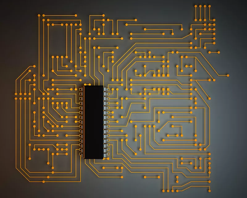
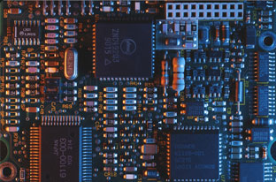
Printed circuit boards (PCBs) are present in nearly all electronic devices. If a piece of equipment contains electronic components, it likely also contains PCBs of various sizes. In addition to housing numerous small parts, the main function of a PCB is to provide electrical connections between these components. As electronic equipment becomes more complex and requires more parts, the wiring and components on the PCB become denser.
The board's substrate is made of an insulated and bend-resistant material, with copper foil serving as the visible surface material. During manufacturing, the entire board is initially covered with copper foil, and the middle part is etched away, leaving behind a network of small lines known as conductors. These conductors are used to provide electrical connections to the parts on the PCB.
To attach parts to the PCB, their pins are soldered directly to the wiring. On a basic PCB, the parts are concentrated on one side, while the wiring is concentrated on the other. Holes are made on the board to allow the pins to pass through to the other side, where they are soldered. This results in the front and back sides of a PCB being referred to as the Component Side and Solder Side, respectively.

PCB Design Basic Knowledge
If there are parts on the PCB that can be removed or reinstalled after manufacturing, sockets are used to install these parts. By directly soldering the socket to the board, the parts can be easily disassembled. A Zero Insertion Force (ZIF) socket allows for easy insertion and removal of parts, with a lever next to the socket holding the parts in place after insertion.
Edge connectors are commonly used to connect two PCBs, with the gold finger containing several bare copper pads that are part of the PCB wiring. To connect, the gold finger on one PCB is inserted into the appropriate slot (commonly called an expansion slot) on the other PCB. In computers, display cards, sound cards, and similar interface cards are connected to the motherboard using a gold finger.
The green or brown color on the PCB indicates the solder mask. This layer serves as an insulating shield, protecting the copper wire and preventing parts from being soldered in the wrong place. Another silk screen printed on the solder resistance layer usually contains words and symbols (mostly white) to indicate the position of the parts on the board.
Single-sided PCBs have parts concentrated on one side and wiring on the other, while double-sided PCBs have wiring on both sides. To use both sides of a double-sided PCB, proper electrical connections between the two sides are necessary. These connections, called guide holes (VIAs), are small holes filled or coated with metal that can be connected to wires on both sides. Due to their ability to accommodate more complex circuits, double-sided PCBs are better suited for such applications than single-sided PCBs.
Why Choose China PCBA Supplier KSPCBA as Your PCB Design Basic Knowledge Manufacturer?
– Experienced and skilled team
– State-of-the-art equipment
– Strict quality control
– Excellent customer service
– Competitive price

Please send Email to kspcba@c-alley.com or call us through +86 13828766801 Or submit your inquiry by online form. Please fill out below form and attach your manufacturing files( PCB Gerber files and BOM List) if need quotation. We will contact you shortly.
 +86 13828766801
 kspcba@c-alley.com
 https://www.kingshengpcba.com/
 2/F, Building 6, Tangtou 3rd Industrial Zone, Tangtou Community, Shiyan Town, Baoan District, Shenzhen, China, 518108