* On your first PCB Assembly order!
* Up to $300 discount
 C - A L L E Y
Home | Events | PCB | About Us | News | Contact Us
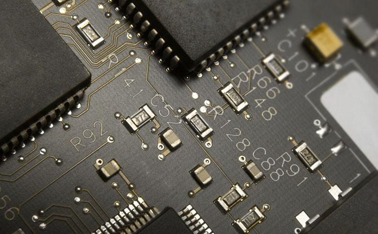
Packaging refers to the circuit pins on a silicon chip that connect to external junctions for integration with other devices. The package form denotes the housing used for installing semiconductor integrated circuit chips. This housing not only serves to install, secure, seal, and protect the chip, but it also enhances thermal performance. The pins of the package connect with wires through contacts on the chip. These pins then connect to other devices via wires on the printed circuit board (PCB), facilitating the connection between the internal chip and the external circuit. It is crucial for the chip to be isolated from the environment to prevent air impurities from corroding the chip’s circuits and degrading electrical performance. Additionally, packaging makes the chips easier to install and transport.
The quality of packaging technology directly affects the chip's performance and the design and manufacturing of the connected PCB. Thus, it is a critical aspect of chip development. A key indicator for assessing the advancement of chip packaging technology is the ratio of chip area to package area; the closer this ratio is to 1, the better.

PCB Electronic Component Packaging Basic Knowledge
Key factors to consider when packaging include:
1. The ratio of chip area to package area should be as close to 1:1 as possible to improve packaging efficiency.
2. The length of the pins should be minimized to reduce delay, while the distance between pins should be maximized to mitigate interference and enhance performance.
3. Based on heat dissipation requirements, thinner packages are generally preferred.
Packages can be mainly categorized into two types: DIP (Dual In-line Package) and SMD (Surface Mount Device). In terms of structure, packaging has evolved from the earliest transistor TO packages (such as TO-89 and TO-92) to the dual-in-line packages and subsequently to SOP (Small Outline Packages) developed by Philips. Over time, various package types have emerged, including SOJ (J-Pin Small Outline Package), TSOP (Thin Small Outline Package), VSOP (Very Small Outline Package), SSOP (Shrink Small Outline Package), TSSOP (Thin Shrink Small Outline Package), SOT (Small Outline Transistor), and SOIC (Small Outline Integrated Circuit).
Materials used in packaging include metal, ceramic, and plastic. Currently, many high-strength applications, such as military and aerospace sectors, still rely on metal packages. The evolution of packaging can be roughly categorized in the following manner:
1. Structure: TO → DIP → PLCC → QFP → CSP
2. Materials: Metal, ceramic → Ceramic, plastic → Plastic
3. Pin Configuration: Long lead in line → Short lead or none → Spherical convex point
4. Assembly Method: Through-hole insertion → Surface mounting → Direct installation with specific package forms.
### Package Types
1. SOP/SOIC Package: SOP stands for Small Outline Package, which was developed by Philips between 1968 and 1969. It has since led to various derivatives like SOJ, TSOP, VSOP, SSOP, TSSOP, SOT, and SOIC.
2. DIP Package: DIP, or Dual In-line Package, is a plug-in type where pins extend from both sides of the package. Made from plastic and ceramic, DIP is commonly used for standard logic ICs, memory LSIs, microcomputers, and more.
3. PLCC Package: PLCC stands for Plastic Leaded Chip Carrier; it is a square package with 32 pins on all sides and is smaller than the DIP package. PLCC is compatible with SMT (Surface Mount Technology), offering advantages of compact size and high reliability.
4. TQFP Package: TQFP stands for Thin Quad Flat Package. This four-sided flat package design efficiently utilizes space, making it suitable for compact applications like PCMCIA cards and networking devices. Almost all of Altera's CPLDs/FPGA products utilize TQFP packages.
5. PQFP Package: PQFP, or Plastic Quad Flat Package, features very small pin distances and thin pins. It's commonly used for large-scale or very large-scale integrated circuits, typically having more than 100 pins.
6. TSOP Packaging: TSOP stands for Thin Small Outline Package, characterized by its small size. A notable feature of TSOP memory packaging is its design, which allows for efficient space usage while maintaining performance.
This comprehensive overview emphasizes the importance of chip packaging in ensuring optimal functionality and integration within electronic devices.
Why Choose China PCBA Supplier KSPCBA as Your PCB Electronic Component Packaging Basic Manufacturer?
– Experienced and skilled team
– State-of-the-art equipment
– Strict quality control
– Excellent customer service
– Competitive price

Please send Email to kspcba@c-alley.com or call us through +86 13828766801 Or submit your inquiry by online form. Please fill out below form and attach your manufacturing files( PCB Gerber files and BOM List) if need quotation. We will contact you shortly.
 +86 13828766801
 kspcba@c-alley.com
 https://www.kingshengpcba.com/
 2/F, Building 6, Tangtou 3rd Industrial Zone, Tangtou Community, Shiyan Town, Baoan District, Shenzhen, China, 518108