* On your first PCB Assembly order!
* Up to $300 discount
 C - A L L E Y
Home | Events | PCBA | About Us | News | Contact Us
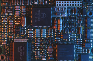
When designing a PCB, it's important to consider the impact of the design on the manufacturing process and the performance of the board. A good PCB design is essential for a qualified hardware engineer and is a key measure of the engineer's overall quality.
Let's discuss the principles of layout design in PCB design and explore the specific requirements in this regard.
1) Ensure that the distance from the edge of the board is greater than 5mm.
2) Prioritize the placement of components closely related to the structure, such as connectors, switches, and power sockets.
3) Place core components and larger components related to circuit function modules first, and then arrange the surrounding circuit electronic components around these core components.

PCB Layout Principles of Design
4) Place high-power electronic components on a circuit board that facilitates heat dissipation. If using a fan for heat dissipation, place it on the main air channel, and if using conductive heat dissipation, place it near the chassis guide slot.
5) Avoid placing high-quality components in the center of the PCB board; instead, position them near the fixed edge of the board in the chassis.
6) Group components with high-frequency connection requirements as much as possible to reduce the distribution parameters of high-frequency signals and electromagnetic interference.
7) Keep input and output components as far away from each other as possible.
8) During debugging, place components with high voltage as securely as possible.
9) Keep thermal components away from heating components to prevent them from being heated and affecting their electrical performance.
10) Ensure that the layout of adjustable components is easy to adjust, such as jumpers, variable capacitors, and potentiometers.
11) Consider the signal flow direction and arrange the layout to maintain a consistent signal flow direction.
12) Ensure that the layout of the PCB circuit board is uniform, neat, and compact.
13) When laying out surface mount components, pay attention to aligning the pad directions as much as possible to facilitate assembly and soldering and reduce the possibility of bridging.
14) Place the decoupling capacitor near the power input terminal.
Why Choose China PCBA Supplier KSPCBA as Your PCB Layout Principles of Design Manufacturer?
– Experienced and skilled team
– State-of-the-art equipment
– Strict quality control
– Excellent customer service
– Competitive price

Please send Email to kspcba@c-alley.com or call us through +86 13828766801 Or submit your inquiry by online form. Please fill out below form and attach your manufacturing files( PCB Gerber files and BOM List) if need quotation. We will contact you shortly.
 +86 13828766801
 kspcba@c-alley.com
 https://www.kingshengpcba.com/
 2/F, Building 6, Tangtou 3rd Industrial Zone, Tangtou Community, Shiyan Town, Baoan District, Shenzhen, China, 518108