* On your first PCB Assembly order!
* Up to $300 discount
 C - A L L E Y
 Home | Events | PCB | About Us | News | Contact Us
1. PCB Size
The size of a printed circuit board (PCB) is limited by the capabilities of the electronic processing production line equipment. Therefore, it is essential to consider the appropriate PCB size during product design.
1. The maximum PCB size that Surface Mount Technology (SMT) equipment can handle is determined by the standard size of PCB sheets, which are typically 20" × 24" (508mm × 610mm).
2. Recommended sizes are based on the specifications of each piece of equipment in the SMT production line, which helps maximize production efficiency and eliminate potential bottlenecks.
3. For smaller PCBs, it is advisable to design them as combinations to enhance overall production efficiency.
Design Requirements:
1. Generally, the maximum PCB size should not exceed 460mm × 610mm.
2. The recommended size range is between 200mm × 250mm and 250mm × 350mm, with a length-to-width ratio of less than 2.
3. For dimensions smaller than 125mm × 125mm, PCBs should be assembled into a more appropriate size.
2. PCB Profile
SMT production equipment uses rails to transport PCBs, and cannot accommodate irregularly shaped PCBs, especially those with notched corners.
Design Requirements:
1. The PCB shape must be a regular square with rounded corners.
2. To ensure stability during transmission, irregularly shaped PCBs should be modified to standard squares, filling corner gaps to avoid jamming during wave soldering.
3. A pure SMT PCB can have a notch, but its size must be less than one-third of the side length where it is located. If this requirement is exceeded, further design modifications are necessary.
4. The chamfer design for gold fingers should include a chamfer on the insertion side, with both sides of the insertion plate also designed with a 1° to 1.5° chamfer at 45° to facilitate insertion.
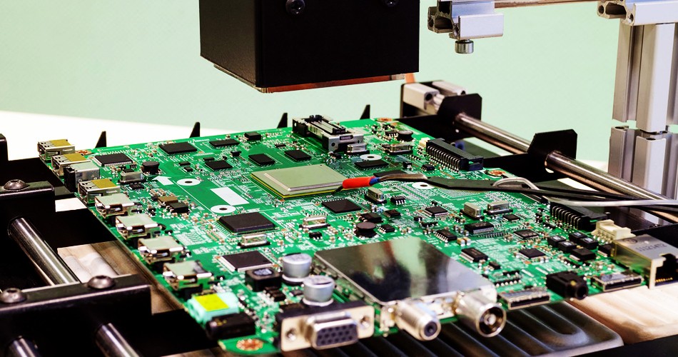
PCBA Processing Automation Production Requirements
3. Transport Side
The transport side's dimensions depend on the requirements of the equipment's transmission guide rail. For the printer, mounting machine, and reflow soldering furnace, the transport side should generally be more than 3.5mm.
Design Requirements:
1. To minimize PCB deformation during soldering, the longer side of the non-assembled PCB should typically be oriented in the direction of transmission. This orientation should also apply to the assembly.
2. Generally, the two edges of the PCB corresponding to the assembly’s transmission direction will serve as the transmission edges. The minimum width for these edges is 5.0mm, and there should be no components or solder joints in front of or behind the transmission edges.
3. There are no restrictions on SMT equipment for the non-transport side. It is advisable to reserve a 2.5mm area for prohibiting element layout.
4. Locating Holes
Accurate PCB positioning is crucial for processes such as plate assembly, assembly, and testing; hence, positioning holes should be designed accordingly.
Design Requirements:
1. Each PCB must have at least two positioning holes: one circular for positioning and the other as a long groove for guidance.
2. There are no specific diameter requirements for the positioning holes; however, recommended diameters are 2.4mm and 3.0mm. The holes should be non-metallic. If the PCB is one that is blanked, a hole plate should be added to enhance rigidity.
3. The length of the guiding hole is typically twice the diameter.
4. The center of each positioning hole should be at least 5.0mm away from the transmission edge, and the two holes should be placed as far apart as possible, preferably in opposite corners of the PCB.
5. For mixed PCBs (with plug-ins installed), the positioning holes should be positioned consistently to allow shared tooling for the front and back, and to accommodate a bottom bracket with screws for the plug-in tray.
5. Locator
Modern equipment such as mounters, printers, optical inspection equipment (AOI), and solder paste inspection equipment (SPI) utilizes optical positioning systems. Therefore, optical positioning symbols must be incorporated into the PCB design.
Design Requirements:
1. Positioning symbols are categorized into global positioning symbols (Global Fiducial) for whole-board positioning and local positioning symbols (Local Fiducial) for assembled sub-boards or fine-pitch components.
2. Optical positioning symbols can be designed in various shapes, such as squares, diamonds, circles, or crosses, with a height of 2.0mm. It is generally recommended to use a circular copper-defined symbol with a diameter of 1.0mm. To ensure contrast with the background material, a non-obstructive soldering area 1mm larger than the optical positioning symbol should be reserved, and no text should be included.
Why Choose China PCBA Supplier KSPCBA as Your PCBA Processing Automation Production Manufacturer?
– Experienced and skilled team
– State-of-the-art equipment
– Strict quality control
– Excellent customer service
– Competitive price
Please send Email to kspcba@c-alley.com or call us through +86 13828766801 Or submit your inquiry by online form. Please fill out below form and attach your manufacturing files( PCB Gerber files and BOM List) if need quotation. We will contact you shortly.
 +86 13828766801
 kspcba@c-alley.com
 https://www.kingshengpcba.com/
 2/F, Building 6, Tangtou 3rd Industrial Zone, Tangtou Community, Shiyan Town, Baoan District, Shenzhen, China, 518108
We would also like to thank our customers for their trust and support. The company's outstanding achievements are mainly due to the loyalty of our customers, which also encourages and spurs our company to forge ahead.