* On your first PCB Assembly order!
* Up to $300 discount
 C - A L L E Y
 Home | Events | PCB | About Us | News | Contact Us
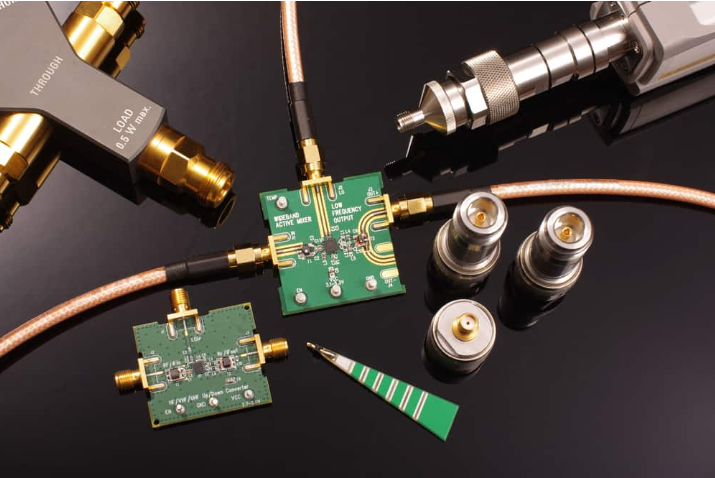
Key Points of Power Supply Design for RF Circuits
The power cord is an important pathway for EMI (Electromagnetic Interference) access to the circuit. Through the power line, external interference can be transmitted to the internal circuit, affecting the performance of RF circuits. To minimize electromagnetic radiation and coupling, the loop area of the primary side, secondary side, and load side of the DC-DC module should be kept to a minimum. Regardless of the complexity of the power circuit, the large current loop should be as compact as possible. It is essential to keep the power cord and ground wire close together.
When using a switching power supply in the circuit, the layout of the peripheral devices should adhere to the principle of the shortest power return path. The filter capacitor should be positioned close to the relevant pins of the switching power supply, and a common mode inductor should be placed near the switching power module.
Power lines that run long distances on a single board should not be located near or pass close to the input and output terminals of a cascade amplifier with a gain greater than 45 dB. This is to prevent power lines from becoming RF signal transmission channels, which can lead to self-excitation or reduced sector isolation. High-frequency filter capacitors are necessary at both ends of long-distance power lines, and even in the middle.
To filter low, medium, and high frequencies on the power line, three filter capacitors should be combined in parallel at the power supply inlet of the RF PCB. For example, use values of 10 µF, 0.1 µF, and 100 pF, arranged in order from large to small and positioned close to the input pins of the power supply.
Power Supply Design of the RF Circuit
When supplying power to small signal cascade amplifiers with the same power source, the power should be supplied sequentially from the last stage to the front stage. This minimizes the impact of EMI generated by the last stage circuit on the previous stage. Each stage of power filtering should include at least two capacitors, such as 0.1 µF and 100 pF. For signal frequencies above 1 GHz, an additional 10 pF filter capacitor should be added.
For low-power electronic filters, the filter capacitor should be placed close to the triode pin, and high-frequency filter capacitors should be positioned even closer to the pin. The triode with the lower cutoff frequency should be selected. If the triode in the electronic filter is a high-frequency tube operating in the amplification region, improper layout of peripheral devices can easily lead to high-frequency oscillations at the power output.
The size of the copper foil in the power section of the PCB must accommodate the maximum current flowing through it, with a general guideline of 1 A/mm line width.
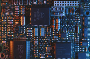
PCB layer allocation simplifies the subsequent wiring process. In a typical four-layer PCB used for WLAN applications, the top layer hosts components and RF leads, the second layer serves as a system layer, the power supply goes on the third layer, and the fourth layer can be used for any signal line distribution.
The second layer should adopt a continuous ground plane layout, which is crucial for establishing an impedance-controlled RF signal path. This layout also facilitates the shortest possible ground loop, providing substantial electrical isolation between the first and third layers to minimize coupling between them. While other layer configurations can be utilized, especially for circuit boards with different layer structures, the aforementioned configuration has proven to be successful.
A large area power supply layer can simplify VCC wiring; however, this structure often introduces noise that degrades system performance. Interconnecting all power leads on a single large plane can exacerbate noise transmission between pins. Alternatively, using star topology significantly reduces coupling between different power supply pins. Implementing effective power decoupling techniques combined with careful PCB layout and a star topology for VCC leads is essential for solid RF system design. While other factors may impact system performance, establishing a "noise-free" power supply is a fundamental element for optimizing overall system performance.
Why Choose China PCBA Supplier KSPCBA as Your Power Supply Design of the RF Circuit Manufacturer?
– Experienced and skilled team
– State-of-the-art equipment
– Strict quality control
– Excellent customer service
– Competitive price
Please send Email to kspcba@c-alley.com or call us through +86 13828766801 Or submit your inquiry by online form. Please fill out below form and attach your manufacturing files( PCB Gerber files and BOM List) if need quotation. We will contact you shortly.
 +86 13828766801
 kspcba@c-alley.com
 https://www.kingshengpcba.com/
 2/F, Building 6, Tangtou 3rd Industrial Zone, Tangtou Community, Shiyan Town, Baoan District, Shenzhen, China, 518108
We would also like to thank our customers for their trust and support. The company's outstanding achievements are mainly due to the loyalty of our customers, which also encourages and spurs our company to forge ahead.
Online Service