* On your first PCB Assembly order!
* Up to $300 discount
 C - A L L E Y
Home | Events | PCBA | About Us | News | Contact Us
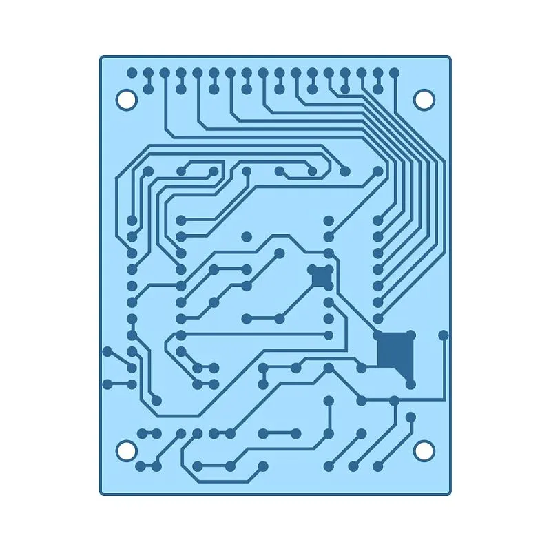
The layout of components on an SMT-PCB is crucial for preventing issues during welding. To avoid drifting or the "tombstone" phenomenon, the long axis of components should be perpendicular to the direction of the conveyor belt on the reflow soldering furnace. Additionally, high-power devices should be evenly dispersed to prevent local overheating, which can impact the reliability of solder joints. When placing components on both sides of the PCB, larger devices should be staggered to avoid affecting the welding process due to increased local heat capacity. Pin-edge devices like PLCC/QFP should not be placed on the wave solder surface. Large SMT devices on the wave soldering surface should have a long axis parallel to the direction of solder wave flow to reduce solder bridging. Finally, small and large SMT components on the wave soldering surface should not be arranged in a straight line but rather staggered to prevent missing soldering due to the "shadow" effect of solder peaks during soldering.

SMT-PCB Design Principles
When placing SMT components on the wave solder surface of an SMT-PCB, the larger components of the pad (such as transistors, sockets, etc.) should have appropriately increased pads. For example, the SOT23 pad can be extended by 0.8-1mm to avoid empty soldering due to the component's "shadow effect." The size of the pad should be determined according to the component's size, with the pad's width equal to or slightly larger than the width of the electrode of the component for the best welding effect. It is essential to avoid using a single large pad between two interconnected components, as the solder on the large pad will connect the two components to the middle. Instead, the correct approach is to separate the two components on the pad and connect them in the middle with a thinner wire. If the wire needs to pass a large current, several wires can be connected in parallel, and the wire is covered with green oil. Finally, it is crucial to avoid placing vias on or near the pads of SMT components, as the solder on the pads will flow down through the vias during the reflow process, resulting in less tin in the solder joints and possibly causing a short circuit on the other side of the board.
Why Choose China PCBA Supplier KSPCBA as Your SMT-PCB Design Principles Manufacturer?
– Experienced and skilled team
– State-of-the-art equipment
– Strict quality control
– Excellent customer service
– Competitive price

Please send Email to kspcba@c-alley.com or call us through +86 13828766801 Or submit your inquiry by online form. Please fill out below form and attach your manufacturing files( PCB Gerber files and BOM List) if need quotation. We will contact you shortly.
 +86 13828766801
 kspcba@c-alley.com
 https://www.kingshengpcba.com/
 2/F, Building 6, Tangtou 3rd Industrial Zone, Tangtou Community, Shiyan Town, Baoan District, Shenzhen, China, 518108