* On your first PCB Assembly order!
* Up to $300 discount
 C - A L L E Y
Home | Events | PCB | About Us | News | Contact Us
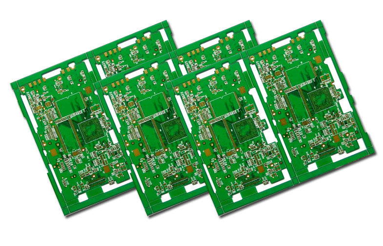
To copy a PCB board, follow these steps:
1. Record the model, parameters, and positions of all vital parts, especially the direction of the diode, the tertiary tube, and the direction of the IC gap. Take two photos of the location of vital parts using a digital camera.
2. Remove all multi-layer boards, copy the boards, and remove the tin in the PAD hole. Clean the PCB with alcohol and put it into the scanner. During scanning, slightly raise the scanned pixels to get a clearer image. Polish the top and bottom layers with water gauze until the copper film is shiny. Then, scan the two layers separately in color and place the PCB horizontally and vertically in the scanner.
3. Adjust the contrast, brightness, and darkness of the canvas to make the part with copper film and the part without copper film have a strong contrast. Turn the second image into black and white and save the pictures as black and white BMP format files TOP.BMP and BOT.BMP.

Specific Steps of PCB Copy Board
4. Convert the two BMP format files into PROTEL format files and transfer them into PROTEL. Ensure that the positions of PAD and VIA after two layers basically coincide. If there are deviations, repeat the previous step.
5. Convert the BMP of the TOP layer to TOP. PCB, pay attention to the conversion to the SILK layer, trace the line on the TOP layer, and place the device according to the drawing. Keep repeating until all the layers are drawn.
6. Import TOP. PCB and BOT. PCB in PROTEL and combine them into one picture.
7. Use a laser printer to print TOPLAYER and BOTTOMLAYER on transparent film (1:1 ratio). Put the film on the PCB and compare whether there are errors. If they are correct, you are done.
To test whether the electronic technical performance of the copy board is the same as the original board, carefully polish the inner layers and repeat the previous steps. Keep in mind that the process may be more complex for multi-layer boards, so special care and attention are required.
Why Choose China PCBA Supplier KSPCBA as Your SMT Chip Processing Process Manufacturer?
– Experienced and skilled team
– State-of-the-art equipment
– Strict quality control
– Excellent customer service
– Competitive price

Please send Email to kspcba@c-alley.com or call us through +86 13828766801 Or submit your inquiry by online form. Please fill out below form and attach your manufacturing files( PCB Gerber files and BOM List) if need quotation. We will contact you shortly.
 +86 13828766801
 kspcba@c-alley.com
 https://www.kingshengpcba.com/
 2/F, Building 6, Tangtou 3rd Industrial Zone, Tangtou Community, Shiyan Town, Baoan District, Shenzhen, China, 518108