* On your first PCB Assembly order!
* Up to $300 discount
 C - A L L E Y
Home | Events | PCBA | About Us | News | Contact Us
What is a multi-layer laminate (BUM-PCB)?
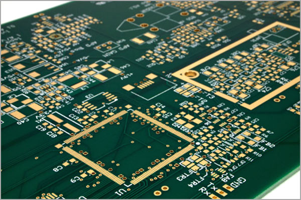
Building Multilayer PCB (BUM) refers to the process of applying insulating dielectric on electro-coated copper and electroplated copper on an insulating substrate or a conventional double-panel or multi-layer board. The connection holes are stacked a plurality of times to accumulate the multilayer printed board that forms the desired number of layers. BUM is designed to meet the requirements of electronic products that are lighter, smaller, thinner, and shorter, and to meet the needs of next-generation electronic packaging technologies (such as BGA, CSP, MCM, FCP, etc.). As a result, it developed very rapidly throughout the 1990s and is mainly used in portable electronic products such as laptops, mobile phones, digital cameras, and MCM package substrates.
In 1998, the global BUM microplate market was worth 1.1 billion US dollars, which rose to nearly 2 billion US dollars in 1999, with 90% of the market concentrated in Japan. The market is expected to be close to 3 billion US dollars in 2000. Domestic experts predict that the world BUM board has entered a development period and that the technological transformation and market competition of the PCB industry will revolve around the BUM board as the center and its surrounding industries (materials, equipment, and testing, etc.) in the next few years.
HDI (high-density interconnect) is the term proposed by European and American countries that corresponds to the Japanese BUM (multilayer laminate). The conceptual connotations of these two nouns are almost the same. According to IPC, the definition of HDI includes the following: non-mechanical drilling aperture is less than 0.15mm (6mil), and most of them are buried holes. The annular ring (pad or land) has a ring diameter of less than 0.25mm (6mil), and a hole that satisfies this condition is called a microtia. A PCB with a micropore has a contact density of 130 points/inch2 or more, and a wiring density (a gorge width channel of 50 mils) at 117 inches/inch2 or above is called an HDI-type PCB. Its line width/line spacing (L/S) is 3 mil/3 mil or less. It can be seen that the most essential feature of the multilayer method is the high-density interconnect (HDI).

Summary of Multilayer Board
Multilayer board manufacturing process
The primary difference between BUM (Build-Up Multilayer) and traditional PCB manufacturing processes is the hole-forming method. Key technologies of BUM include the selection of dielectric materials used in the laminated insulation layer, the microporous hole-forming technology, and the hole metallization technology.
There are several different BUM manufacturing methods due to the variation in insulating layer materials and interconnected micropore processing methods. However, mature processes can be mainly classified into three types: resin-coated copper foil (RCC), thermosetting resin (dry film or liquid), and photosensitive resin (dry film or liquid). The latter two processes generally require metallization and line formation through an additive process, which is highly demanding on materials and corresponding technologies.
The RCC process, on the other hand, uses the subtractive process to complete circuitization. It does not require a large equipment investment (the main investment is a laser driller) and is adaptable to the traditional multilayer PCB manufacturing process. The finished BUM board has good performance and reliability. There is an increasing demand for RCC technology, and more and more manufacturers are using it to produce BUM boards. However, the build layer of the BUM on the core board generally does not exceed four layers due to the limitation in flatness of the board surface.
Why Choose China PCBA Supplier KSPCBA as Your Multilayer Board Manufacturer?
– Experienced and skilled team
– State-of-the-art equipment
– Strict quality control
– Excellent customer service
– Competitive price

Please send Email to kspcba@c-alley.com or call us through +86 13828766801 Or submit your inquiry by online form. Please fill out below form and attach your manufacturing files( PCB Gerber files and BOM List) if need quotation. We will contact you shortly.
 +86 13828766801
 kspcba@c-alley.com
 https://www.kingshengpcba.com/
 2/F, Building 6, Tangtou 3rd Industrial Zone, Tangtou Community, Shiyan Town, Baoan District, Shenzhen, China, 518108