* On your first PCB Assembly order!
* Up to $300 discount
 C - A L L E Y
Home | Events | PCBA | About Us | News | Contact Us
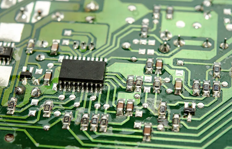
With the rapid development of the social economy, various electronic devices continue to emerge, and some of these devices rely on electronic components. Thus, understanding the installation process of PCB boards is crucial. First, it is important to assess the structure of the circuit board, especially for wires and tubes with significant structural rigidity, as they can be challenging to work with.
The first step is to apply solder paste. This step ensures that the SMD components and the corresponding pads of the PCB achieve a good electrical connection and have sufficient mechanical strength during reflow soldering. Solder paste is a mixture of alloy powder, paste flux, and some additives with a certain viscosity and good touch characteristics. It is necessary to evenly place an appropriate amount of solder paste on the PCB pads to ensure good electrical connection and mechanical strength.

The Process Flow of PCB Board Placement
The second step involves mounting components on the PCB board. This process accurately mounts the chip components to the corresponding positions on the PCB surface where the solder paste or patch glue is printed, using a placement machine or manual placement. Machine placement is suitable for large batches and tight supply cycles, albeit with complicated working procedures and large investments. On the other hand, manual placement is suitable for small to medium batch production and product development, offering easy operation and low cost, but the production efficiency relies on the proficiency of operators.
The third step is the PCB board patch reflow soldering, which involves remelting the solder paste pre-distributed on the printed board pad to achieve the mechanical and electrical connection between the solder end of the surface mount component or the pin and the printed board pad. This process is crucial, and each step should be carried out meticulously to ensure orderly placement work.
Why Choose China PCBA Supplier KSPCBA as Your PCB Board Placement Manufacturer?
– Experienced and skilled team
– State-of-the-art equipment
– Strict quality control
– Excellent customer service
– Competitive price

Please send Email to kspcba@c-alley.com or call us through +86 13828766801 Or submit your inquiry by online form. Please fill out below form and attach your manufacturing files( PCB Gerber files and BOM List) if need quotation. We will contact you shortly.
 +86 13828766801
 kspcba@c-alley.com
 https://www.kingshengpcba.com/
 2/F, Building 6, Tangtou 3rd Industrial Zone, Tangtou Community, Shiyan Town, Baoan District, Shenzhen, China, 518108