* On your first PCB Assembly order!
* Up to $300 discount
 C - A L L E Y
Home | Events | PCB | About Us | News | Contact Us
With advancements in microelectronics technology and industrial manufacturing, printed circuit boards (PCBs) have become fundamental components in all smart devices and systems. PCBs facilitate wiring and electrical connections between various electronic components, such as integrated circuits. They provide insulation, ensuring the necessary electrical characteristics, as well as solder mask graphics for automatic soldering and identification markings for component insertion, inspection, and maintenance.
### 1. General Steps in PCB Design
The design of a printed circuit board is based on the circuit schematic diagram, aimed at fulfilling the functions required by the user. The PCB design primarily involves layout planning, which encompasses the arrangement of internal components, metal wiring, through-holes, and external connections. Important considerations in this process include point protection, heat dissipation, and crosstalk. An excellent circuit design can reduce production costs while achieving optimal circuit performance and thermal management. Simple layouts can be completed manually, whereas more complex designs generally require the use of computer-aided design (CAD) tools.
Popular design software includes OrCAD, Pads (PowerPCB), Altium Designer, FreePCB, and others. During PCB design, it is essential to accurately specify the pin size and structural package details of all components. It’s important to note that even among components of the same type from different manufacturers, variations in values and pin arrangements may exist.
Next, based on the designed electrical schematic, the overall block diagram of the components is simulated. Finally, in the sketch of the circuit board, the detailed pins of each component must be drawn, along with their positions. Care should be taken to consider the sizes of the components, the distance between them, and the placement of peripheral components relative to the edges, as well as input and output connections, grounding, power lines, and high-frequency and signal lines susceptible to radiation and interference.

The Specific Steps And Composition of PCB
### 2. Composition of PCBs
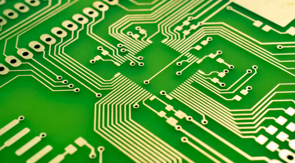
1. **Lines and Artwork (Pattern):** The lines serve as the conductive paths for the components. In the design, larger copper surfaces, known as grounding and power layers, are also incorporated. The lines and artwork are created simultaneously.
2. **Dielectric Layer:** This layer maintains insulation between lines and layers and is commonly referred to as the substrate.
3. **Through Holes / Vias:** Vias enable connections between lines on different levels. Larger vias are used for component insertion, while non-conductive holes (nPTH) are typically used for surface mount positioning and as fasteners during assembly.
4. **Solder Resist Ink (Solder Mask):** Not all copper surfaces require solder; therefore, non-soldered areas are coated with a material (usually epoxy resin) that prevents solder from adhering, thereby avoiding short circuits. This layer can be differentiated by color, often referred to as "green oil," "red oil," or "blue oil," depending on the process used.
5. **Silkscreen (Legend / Marking):** This is a non-essential component that primarily serves to label the names and positions of each part on the circuit board for easier maintenance and identification after assembly.
6. **Surface Finish:** Copper surfaces are prone to oxidation, which can negatively affect solderability; thus, protective coatings are applied. Methods include HASL, ENIG, Immersion Silver, Immersion Tin, and OSP. Each method has its own advantages and disadvantages, grouped under the term "surface treatment."
The PCB production process is complex and involves a range of procedures, from simple to intricate mechanical processing, as well as chemical, photochemical, electrochemical, and thermochemical techniques, alongside computer-aided design (CAM) knowledge. Numerous technological challenges can arise during production, often with new issues surfacing unexpectedly, while others may resolve themselves without understanding the underlying causes. Given that the production process operates on a discontinuous assembly line, any problem at any stage can halt production or lead to significant scrap. Unfortunately, once a printed circuit board is scrapped, it cannot be recycled or reused. Consequently, process engineers face considerable pressure, which often leads many to transition into roles with PCB equipment or material suppliers, focusing on sales and technical services.
Why Choose China PCBA Supplier KSPCBA as Your The Specific Steps And Composition of PCB Manufacturer?
– Experienced and skilled team
– State-of-the-art equipment
– Strict quality control
– Excellent customer service
– Competitive price

Please send Email to kspcba@c-alley.com or call us through +86 13828766801 Or submit your inquiry by online form. Please fill out below form and attach your manufacturing files( PCB Gerber files and BOM List) if need quotation. We will contact you shortly.
 +86 13828766801
 kspcba@c-alley.com
 https://www.kingshengpcba.com/
 2/F, Building 6, Tangtou 3rd Industrial Zone, Tangtou Community, Shiyan Town, Baoan District, Shenzhen, China, 518108