* On your first PCB Assembly order!
* Up to $300 discount
 C - A L L E Y
Home | Events | PCBA | About Us | News | Contact Us
1. SMT
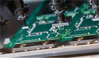
Surface mount technology, also known as SMT, is classified into two categories: no leads and short leads. It is a technique for assembling circuits that uses dip or reflow soldering to join components. Additionally, it is the most widely used in the electronics assembly sector. a combination of craftsmanship and technology.
Features of SMT: The substrate of a PCB can be utilized for structure, heat dissipation, power supply, and signal transmission.
SMT characteristics: able to tolerate the temperature and time of curing and soldering. The flatness satisfies the manufacturing process's criteria. ideal for reworking tasks. appropriate for the substrate's manufacturing process. Both high resistance and low dielectric count. Epoxy resins and phenolic resins, which are inexpensive, have good mechanical and dielectric qualities, good temperature characteristics, good flame resistance, and are environmentally benign, are the materials that are frequently utilized for our product substrates. The solidification of the stiff substrate is indicated above. Additionally, our products feature flexible substrates that can be folded, turned, and moved to conserve space. They operate well at high frequencies and are composed of extremely thin insulating sheets.
The challenging assembling procedure and incompatibility for fine-pitch applications are the drawbacks. Small leads and spacing, huge thickness and area, improved heat conductivity, tougher mechanical qualities, and improved stability are, in my opinion, the substrate's qualities. In my opinion, standard parts, electrical performance, and dependability make up the substrate mounting method. We offer the dual guarantee of manual review, machine review, and manual review in addition to fully automated and integrated operation. Product qualification rate for IPCB is up to 99.98%.

2. PCB
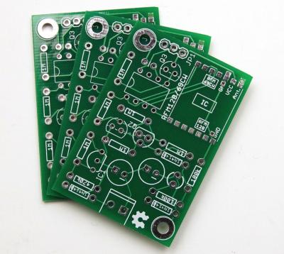
One of the most crucial electronic parts is the PCB. Generally speaking, a printed circuit is a conductive pattern created on an insulating material in accordance with a predefined design using printed circuits, printed components, or a combination of the two. A printed circuit board, also known as a printed circuit board, is a conductive pattern that creates electrical connections between components over an insulating substrate. It serves as a carrier for components and an essential support for electronic components.
When we open a computer keyboard, we typically observe a piece of soft film, which is a flexible insulating substrate printed with healthy bit patterns and silver-white, or silver paste, conductive patterns. We refer to this type of printed circuit board as a flexible silver paste printed circuit board since it is produced using the standard screen printing technique.
Every motherboard, graphics card, network card, modem, sound card, and home appliance that we observed in Computer City had a different printed circuit board. The substrate used in it is made of a paper base (usually used for single-sided) or glass cloth base (usually used for double-sided and multilayer), pre-impregnated phenolic or epoxy resin, one or both sides of the surface layer is glued with copper-clad sheets and then laminated to cure Become. This type of circuit board is known as a rigid board since it is made of copper-clad sheet material. Create a printed circuit board after that; this is known as a rigid printed circuit board. Printed circuit boards with printed circuit patterns on one side and printed circuit boards with printed circuit patterns on both sides are referred to as single-sided printed circuit boards. Double-sided boards are printed circuit boards created by double-sided connections via hole metallization. The positioning system and the insulating bonding material alternate together, and the printed circuit board with the conductive pattern interconnected by the design requirements becomes a four-layer or six-layer printed circuit board, also known as a multilayer printed circuit board, if one double-sided as the inner layer, two single-sided as the outer layer, or two double-sided as the inner layer and two single-sided as the outer layer.

3. PCBA
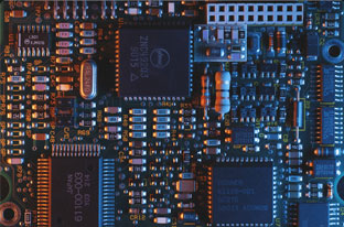
The term "PCBA process" refers to the entire surface mount technology (SMT) and DIP plug-in insertion process for PCBs. It's a PCB with a repair on it. A finished board is one, and a naked board is the other. A PCBA is a completed circuit board; that is, a circuit board that has undergone all of its necessary processing to be considered finished. Owing to the ongoing reduction in size and improvement of electronic goods, etching resists—either laminated or coated—are used to attach most circuit boards nowadays. Etching is used to create the circuit boards following exposure and development.
Because of the low PCBA assembly density in the past and the widespread belief that the flux residue was benign, non-conductive, and would not impair electrical performance, cleaning expertise was insufficient. Electronic assemblies of today are typically smaller, even tiny devices or pitches. Pins and pads are drawing nearer together. These days, the gap is getting increasingly smaller, and pollutants could become lodged there. This implies that the particles between the two gaps might still be rather small, an unwanted occurrence that results in a short circuit.
The electronics assembly sector has been advocating for and becoming more conscious of cleaning in recent years, not just for products but also for environmental regulations and public health. As a result, there are numerous companies offering cleaning solutions and equipment, and in the electronics assembly sector, cleaning is now a common topic of conversation and technical exchanges.

4. DIP
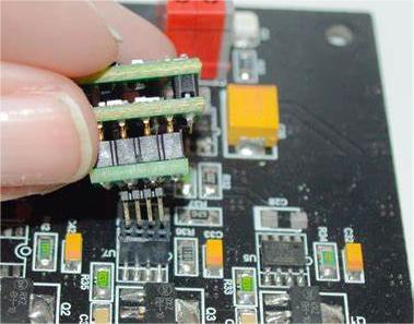
Dual in-line packaging, or DIP, is the term used to describe integrated circuit chips that are packaged in dual in-line configurations. Most tiny and medium-sized integrated circuits adopt this packaging style as well, and typically have no more than 100 pins. The two rows of pins on a CPU chip that uses DIP packaging technology must fit into a chip socket that also has a DIP configuration. Naturally, it can also be put straight into a circuit board that has the same amount of solder holes and soldering orientation. To prevent pin damage when plugging and unplugging from the chip socket, DIP packaging technique users should exercise extra caution.
DIP's features include lead frame DIP (which includes glass ceramic sealing type, plastic encapsulation structure type, and ceramic low-melting glass packaging type), multilayer ceramic double in-line DIP, and single-layer ceramic double in-line DIP.
A link in the electronic manufacturing process is the DIP plug-in. AI machine plug-ins and manual plug-ins are both available. Insert the provided item into the specified place. The electronic components on the board must be soldered using wave soldering, which is a laborious process. Verify if the components have been correctly put or if any are missing. One crucial step in processing PCBA patches is the DIP plug-in post-welding procedure. The PCBA board's functionality is directly impacted by the quality of its processing, so it is crucial. Subsequent post-welding is necessary because some components can only be manually welded due to limitations in materials and technique when using a wave soldering machine. This illustrates the significance of DIP plug-ins in electronic parts as well. It can only be flawless if you pay close attention to the details.


Please send Email to kspcba@c-alley.com or call us through +86 13828766801 Or submit your inquiry by online form. Please fill out below form and attach your manufacturing files( PCB Gerber files and BOM List) if need quotation. We will contact you shortly.
 +86 13828766801
 kspcba@c-alley.com
 https://www.kingshengpcba.com/
 2/F, Building 6, Tangtou 3rd Industrial Zone, Tangtou Community, Shiyan Town, Baoan District, Shenzhen, China, 518108