* On your first PCB Assembly order!
* Up to $300 discount
 C - A L L E Y
Home | Events | PCBA | About Us | News | Contact Us
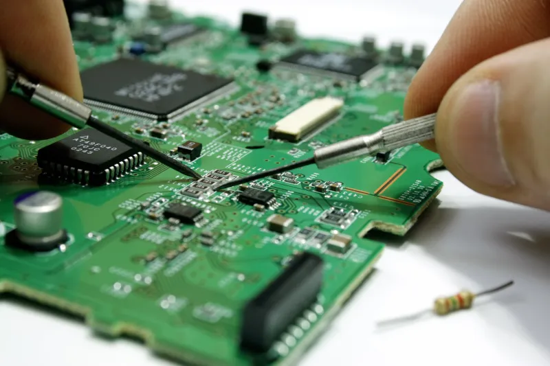
When processing PCBA welding, there are several requirements for the PCBA board. The board must meet these requirements to undergo the welding process. Why are so many requirements needed for the welding process? This is because PCBA processing involves many special processes, which demand specific requirements for the PCB board. If there are any issues with the PCB board, it can increase the difficulty of the PCBA soldering process, resulting in welding defects and unqualified boards. Therefore, to ensure the smooth completion of the special process and to facilitate the PCBA soldering process, the PCB board must meet the manufacturability requirements in terms of size and pad distance.
Here are the requirements for the PCBA welding process for PCB boards:
1. PCB size: The width of the PCB (including the edge of the board) should be greater than 50mm and less than 460mm. The length of the PCB (including the edge of the board) should be greater than 50mm. If the size is too small, it needs to be made into a jigsaw.
2. PCB board edge width: The board edge width should be greater than 5mm, the panel spacing should be less than 8mm, and the distance between the pad and board edge should be greater than 5mm.

Welding Processing Requirements for PCBA
3. PCB bending: The upward bending degree should be less than 1.2mm, the downward bending degree should be less than 0.5mm, and the PCB distortion should be maximum deformation height ÷ diagonal length < 0.25.
4. PCB board mark point: The mark shape should be a standard circle, square, or triangle, and the mark size should be 0.8~1.5mm. The mark material should be gold-plated, tin-plated, copper, or platinum, and the mark's surface should be flat, smooth, non-oxidized, and free of dirt. The mark's surrounding requirements state that there should be no green oil or other obstacles within 1mm, which is different from Mark's color. The mark position should be 3mm above the edge of the board, and there should be no Mark-like vias, test points, etc. within 5mm around the board.
5. PCB pads: There should be no through holes on the pads of SMD components. If there is a through the hole, the solder paste will flow into the hole, resulting in less tin in the device, or the tin flowing to the other side, causing the board surface to be uneven, and the solder paste cannot be printed.
When designing and producing PCBs, it is essential to understand the PCBA welding process to ensure that the product is suitable for production. Understanding the requirements of the processing plant can make the subsequent manufacturing process smoother and avoid unnecessary troubles.
These are the requirements for the PCBA welding process for PCB boards. When producing PCB boards, do not slacken your efforts. Only by producing high-quality and compliant PCB boards can the board better accept other special processes, inject the soul of function, and give the PCB board life.
Why Choose China PCBA Supplier KSPCBA as Your Welding Processing Requirements for PCBA Manufacturer?
– Experienced and skilled team
– State-of-the-art equipment
– Strict quality control
– Excellent customer service
– Competitive price

Please send Email to kspcba@c-alley.com or call us through +86 13828766801 Or submit your inquiry by online form. Please fill out below form and attach your manufacturing files( PCB Gerber files and BOM List) if need quotation. We will contact you shortly.
 +86 13828766801
 kspcba@c-alley.com
 https://www.kingshengpcba.com/
 2/F, Building 6, Tangtou 3rd Industrial Zone, Tangtou Community, Shiyan Town, Baoan District, Shenzhen, China, 518108