* On your first PCB Assembly order!
* Up to $300 discount
 C - A L L E Y
Home | Events | PCBA | About Us | News | Contact Us
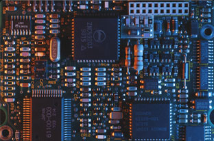
The circuit board refers to the use of Electronic Design Automation software (EDA) to design the circuit board and layout the connections of the printed circuit board (PCB). The design of the PCB mainly involves layout design, considering the layout of external connections, the optimized layout of internal electronic components, metal connections, through-holes, electromagnetic protection, and thermal dissipation. Circuit boards are crucial in electronic products as they connect electronic components and transmit signals through wires.
How to design a PCB?
Designing a PCB involves different point settings at different stages. Large grid points can be used for device layout during the layout stage. A grid accuracy of 50-100 mils can be selected for large devices such as ICs and non-positioning connectors, while a grid accuracy of 25 mils can be used for passive small devices such as resistors, capacitors, and inductors. The accuracy of large grid points is beneficial for device alignment and layout aesthetics.

What is PCB design?
PCB layout rules:
1) All components should generally be arranged on the same side of the circuit board. Top layer components can be placed on the bottom layer only if the top layer components are too dense, and limited and low heat-generating devices, such as chip resistors, chip capacitors, and chip ICs, can be placed.
2) Components should be placed on a grid and arranged parallel or perpendicular to each other, ensuring neatness and beauty. Overlapping of components is generally not allowed, and the arrangement should be compact, with components evenly and densely distributed throughout the entire layout.
3) The minimum spacing between adjacent solder pad patterns of different components on the circuit board should be at least 1mm.
4) The distance from the edge of the circuit board should generally not be less than 2mm. The best shape of the circuit board is rectangular, with an aspect ratio of 3:2 or 4:3. For circuit boards larger than 200mm by 150mm, mechanical strength should be considered.
Special components in PCB:
Special components refer to key components in the high-frequency part, core components in the circuit, easily disturbed components, components with high voltage, components with high heat generation, and some heterogeneous components. The positions of these special components need to be carefully analyzed, and their layout should meet the requirements of circuit functions and production needs. Improper placement of these components may cause circuit compatibility and signal integrity problems, leading to PCB design failure.
PCB design is crucial for achieving electronic system functions. If the PCB design is not reasonable, the functionality of the entire electronic system will be affected. PCB design can help control the parameters of electronic components, such as power, signal, and power supply. It can also help control the quality of electronic products, thereby improving product reliability and safety.
Why Choose China PCBA Supplier KSPCBA as Your PCB design Manufacturer?
– Experienced and skilled team
– State-of-the-art equipment
– Strict quality control
– Excellent customer service
– Competitive price

Please send Email to kspcba@c-alley.com or call us through +86 13828766801 Or submit your inquiry by online form. Please fill out below form and attach your manufacturing files( PCB Gerber files and BOM List) if need quotation. We will contact you shortly.
 +86 13828766801
 kspcba@c-alley.com
 https://www.kingshengpcba.com/
 2/F, Building 6, Tangtou 3rd Industrial Zone, Tangtou Community, Shiyan Town, Baoan District, Shenzhen, China, 518108