* On your first PCB Assembly order!
* Up to $300 discount
 C - A L L E Y
About Us | Events | Company Structure | Management Staff Structure | Market Focus | Company Certification | Our Services
Definitions:
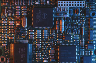
For standard PCB, it is the combination of bare board and components on it. While for bare board PCB, it is called printed wiring board. We usually call it PWB.
(1) Traces:
The base material of PCB is comprised of dielectric, heat insulation, uneasy to bend materials.
On its surface, we can see thin traces, its material is copper. Originally the copper covered the whole PCB.
Parts of it were etched during the process of production. Those parts left become net-like thin traces,
which are called conductor pattern, and are used to provide circuit connection for components on PCB.
(2) Name of two side:
On most common single sided PCB, components are on one side, conductor pattern is on the other side.
Then we would need to drill holes on the board, so that pins can put through the board to the other side.
Therefore, the both sides of PCB are called component side and solder side.
(3) Gold finger:
Gold finger is functioned to connect two PCBs. We usually insert the gold finger of one PCB to the proper slot of the other PCB.
(4) Solder mask and silk screen:
The green or white oil on PCB is called solder mask, which is functioned as dielectric protective layer, can protects copper traces and also can prevent components to be soldered at incorrect place.
On the dielectric layer, a layer of silk screen will be printed. Some words will be printed to show the position of those components. It is also called legend.

Please send Email to kspcba@c-alley.com or call us through +86 13828766801 Or submit your inquiry by online form. Please fill out below form and attach your manufacturing files( PCB Gerber files and BOM List) if need quotation. We will contact you shortly.
 +86 13828766801
 kspcba@c-alley.com
 https://www.kingshengpcba.com/
 2/F, Building 6, Tangtou 3rd Industrial Zone, Tangtou Community, Shiyan Town, Baoan District, Shenzhen, China, 518108