* On your first PCB Assembly order!
* Up to $300 discount
 C - A L L E Y
About Us | Events | Company Structure | Management Staff Structure | Market Focus | Company Certification | Our Services
This artical is introducing what is PCB assembly. If you have any demand for pcba, pls contact with us freely.
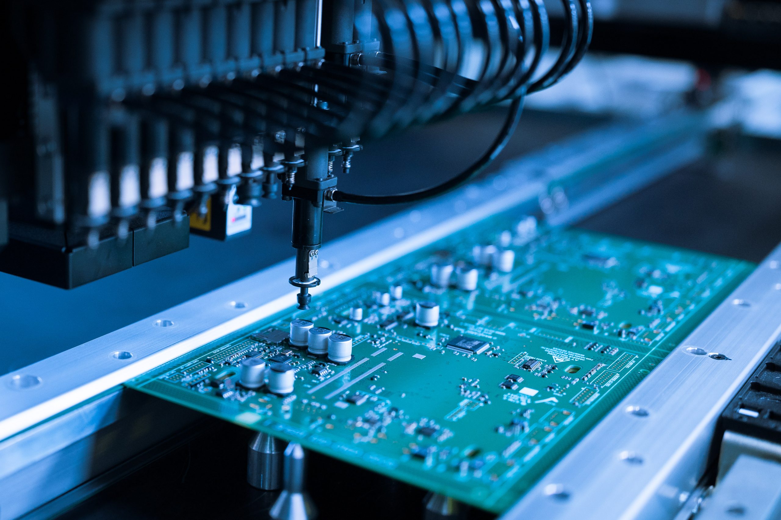
In assembly the bare board is populated with electronic components to form a functional printed circuit assembly (PCA), sometimes called a "printed circuit board assembly" (PCBA). In through-hole technology component leads are inserted in holes. In surface-mount technology (SMT) the components are glued on pads or lands on the surfaces of the PCB. In both component leads are then mechanically fixed and electrically connected to the board by soldering.
There are a variety of soldering techniques used to attach components to a PCB. High volume production is usually done with SMT placement machine and bulk wave soldering or reflow ovens, but skilled technicians are able to solder very tiny parts (for instance 0201 packages which are 0.02 in. by 0.01 in.) by hand under a microscope, using tweezers and a fine tip soldering iron for small volume prototypes. Some parts may be extremely difficult to solder by hand, such as BGA packages.
Often, through-hole and surface-mount construction must be combined in a single assembly because some required components are available only in surface-mount packages, while others are available only in through-hole packages. Another reason to use both methods is that through-hole mounting can provide needed strength for components likely to endure physical stress, while components that are expected to go untouched will take up less space using surface-mount techniques. For further comparison, see the SMT page.

After the board has been populated it may be tested in a variety of ways:
While the power is off, visual inspection, automated optical inspection. JEDEC guidelines for PCB component placement, soldering, and inspection are commonly used to maintain quality control in this stage of PCB manufacturing.
While the power is off, analog signature analysis, power-off testing.
While the power is on, in-circuit test, where physical measurements (for example, voltage) can be done.
While the power is on, functional test, just checking if the PCB does what it had been designed to do.
To facilitate these tests, PCBs may be designed with extra pads to make temporary connections. Sometimes these pads must be isolated with resistors. The in-circuit test may also exercise boundary scan test features of some components. In-circuit test systems may also be used to program nonvolatile memory components on the board.
In boundary scan testing, test circuits integrated into various ICs (BQFP, BGA, LGA, DIP and so on. ) on the board form temporary connections between the PCB traces to test that the ICs are mounted correctly. Boundary scan testing requires that all the ICs to be tested use a standard test configuration procedure, the most common one being the Joint Test Action Group (JTAG) standard. The JTAG test architecture provides a means to test interconnects between integrated circuits on a board without using physical test probes. JTAG tool vendors provide various types of stimulus and sophisticated algorithms, not only to detect the failing nets, but also to isolate the faults to specific nets, devices, and pins.
When boards fail the test, technicians may desolder and replace failed components, a task known as rework.
Our company Kingsheng PCBA tech. is providing with OEM pcb assembly service, we have X-ray and AOI matchine, can do assembly for high precision components like BGA and 01005. If you have any project need us quote to you, please contact with us freely.

Please send Email to kspcba@c-alley.com or call us through +86 13828766801 Or submit your inquiry by online form. Please fill out below form and attach your manufacturing files( PCB Gerber files and BOM List) if need quotation. We will contact you shortly.
 +86 13828766801
 kspcba@c-alley.com
 https://www.kingshengpcba.com/
 2/F, Building 6, Tangtou 3rd Industrial Zone, Tangtou Community, Shiyan Town, Baoan District, Shenzhen, China, 518108