* On your first PCB Assembly order!
* Up to $300 discount
 C - A L L E Y
About Us | Events | Company Structure | Management Staff Structure | Market Focus | Company Certification | Our Services
KingshengPCBA (www.kingshengpcba.com) is an ISO certifiled electronic contract manufacturer of complex PCB assemblies announces the install of automatic optical inspection (AOI ) system to their facility . KingshengPCBA specialises in manufacturing of high reliable electric products for Medici ,Avionics, Defense, and Commercial industries.
KingshengPCBA institute the most technically advanced manufacturing practices and equipment in the industry and continue to invest in major equipment purchases to keep up with their surging customer demand for manufacturing assembly services.
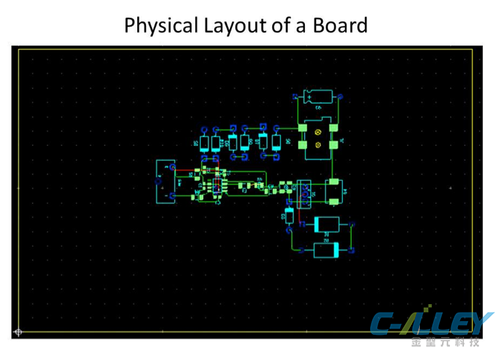
Board layout takes prototype design to a whole new level of achievement. Whereas this was once a trait limited to designated personnel and high-priced software packages, it is now a free and downloadable software from the internet. This frees you from the confines of your cubicle to use at home via your ISP. One benefit is the fact that any circuits you develop are not the property of your employer if you use your own computer. Other legal restrictions may apply including your Employee Agreement as well as whether your employer reimburses you for internet fees. Always understand these limitations before venturing off to invent the next greatest gizmo.
Board layout is often a compromise between component size, generated heat, and signal routing. All of these factors play a part in the final layout. However, one must also consider the final populating of the board. That is why it is good to get involved with your prototyping house early on. Everything from kitting to special connections could affect your prototype. For example, putting a heavy magnetic component on a flexible circuit board may not be your best move. Therefore, have some foresight with your board stuffing house as you did between your schematic and the board layout.
Physical board layout for bench top prototype analysis focuses on the X and Y axis. Components lie in a north-south direction or east-west direction along with axis. Leave plenty of room for extra components and accessing crucial signals. Unused components can be unpopulated or shorted depending on the need. Therefore, using 0 ohm resistors for shorts in your schematic might be a good idea Or, putting in an extra lot of unpopulated compensation components could save adding elevated components in the future.
In the same manner you populate for components, think in advance of how the components are packaged. As surface mount overtakes leaded components, it's best to have a prototype house wave solder the package rather than waiting until you can do it yourself after the board arrives. As components shrink and increase in integration, there are certain jumping off points that you must consider and prepare for. Consider time saving measures in advance especially if you have a client deadline.
For those prototypes that are going into an assembly or fixture, the Z direction must be considered if height is an issue. Also, these designs will most likely be more compact than their bench top counterparts. Connectors such as USB interfaces work better as edge mounted components that align with access holes on the case. Similarly, consider any power jacks, LED indicators, or audio jacks as well.

After using Ultiboard by National Instruments, I have mixed feelings. Overall, this is a great tool as it does a lot of thinking for you. There are some frustrations involved as the screen size makes it difficult to move components. I often had to zoom into a point where I could grab the component. The problem was, the area where I wanted to place the component was now outside my field of vision. If I zoomed out further I would get scolded for grabbing a component pad rather than the component itself. This is something to think about if you are lying in bed looking at a notebook screen rather than at your desk with a larger view of multiple screens.
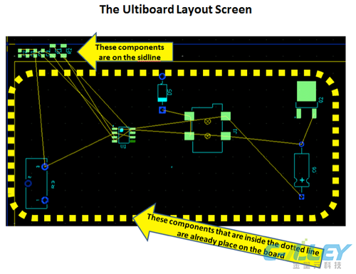
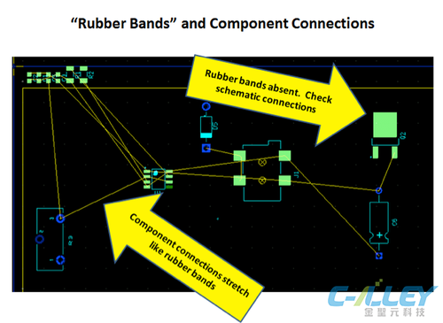
After moving a few components, it is apparent that some of them are on the board while others are on the sideline waiting to get into the game (as shown). All components start on the sideline and have to be moved onto the board. It helps if you have a view of your schematic available when placing components. This will be a vital part of the routing step in order to reduce signal interference, grounding effects, and sharing the heat generated by individual components.
What is nice about this software as it has a "nudging" feature that moves placed components when you are placing a selected component. This feature is adjustable with a selectable variable that controls component spacing.


Please send Email to kspcba@c-alley.com or call us through +86 13828766801 Or submit your inquiry by online form. Please fill out below form and attach your manufacturing files( PCB Gerber files and BOM List) if need quotation. We will contact you shortly.
 +86 13828766801
 kspcba@c-alley.com
 https://www.kingshengpcba.com/
 2/F, Building 6, Tangtou 3rd Industrial Zone, Tangtou Community, Shiyan Town, Baoan District, Shenzhen, China, 518108