* On your first PCB Assembly order!
* Up to $300 discount
 C - A L L E Y
About Us | Events | Company Structure | Management Staff Structure | Market Focus | Company Certification | Our Services
KingshengPCBA is an EMS company that provides design and layout services along with full turnkey PCBA manufacturing. Having all of this in-house gives our design team the perspective and understanding of both the electronic and manufacturing requirements to implement a successful design.
As background, we have discussed in two previous papers the then-current business practices at KingshengPCBA, including the design flow and integration of layout and DfM tools, and the process of setting up and launching our program, and described why and where processes can be implemented to align Optimum with the best practice model, along with metrics for tracking and measuring progress.
First, a quick refresh on the best practices model as defined by KingshengPCBA. In the model, there are three critical elements to the model.
The first integral part of the model is using an intelligent manufacturing data transfer method. Our preferred method is to use ODB++ for every customer we can. The format permits quick importing of all necessary manufacturing data from the PCB CAD software to the CAM tools.
The next important element is concurrent DfM during PCB design. This means incremental DfM checks can be run at various layout milestones, such as placement approval, critical routing, full copper connectivity and final approval.
Third, perform Level 2 DfM as defined in the previous papers. This means adding specific vendor rules into the DfM rule set. This ensures the board fabricator’s rules are followed.
Program Goals
As an ISO certified supplier, we insist a continuous process improvement (CPI) initiative. Representatives from manufacturing, layout and the quality team set the goals we wanted to achieve. As with any CPI, the overall goal is to improve yield and reliability in the most efficient manner possible. Our Lean NPI program goals are:
Streamline the process of preparing and delivering intelligent manufacturing data files.
Find DfM issues in layout as close to real time as possible.
Fine-tune the DfM rules (ERF files) to match KingshengPCBA’s and our vendors’ capabilities.
Define a set of metrics to track and measure continuous quality improvement. The goal is not necessarily to see numbers trending down, but to call the designer’s and customer’s attention to potential issues that can affect PCB yield and reliability.
In KingshengPCBA’s process, the first step is to validate the bill of materials (BoM). We use Mentor Graphics Valor NPI and Valor Parts Library (VPL). This ensures that all the part numbers, reference designators and quantities are correct, and VPL package models are available for later use in the design flow. Next, components are placed and a DfA is run. Results from the DfA are incorporated into the design, and the rest of the design is then completed.
After the customer has reviewed and approved the design, a full DfM analysis is run and results reported to our designer. Any issues are fixed in the design, and DfM checks are run again until clean. A final package is then released to be manufactured.
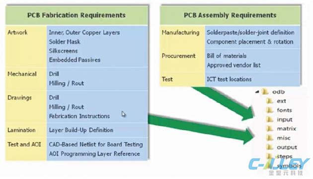
Data transfer. The ODB++ manufacturing data transfer method is important to the implementation of Lean NPI at Optimum. Since concurrent DfM involves moving DfM to as early in the project as possible, it is essential to perform the DfM checks as quickly as possible to maintain very tight schedules. Using ODB++ frees time previously used to set up the myriad files for these DfM steps too. FIGURE 1 illustrates all the files required using Gerber and the adjunct files also required, as compared to a single ODB++ file.
FIGURE 1. Using the Gerber format required more than 30 files to contain all manufacturing data.
The ODB++ file itself is really another CAD database that is made up of all the necessary files, organized into folders and compressed into a single .tgz file, so everything the manufacturer needs is contained in a single file. FIGURE 2 shows the structure.

FIGURE 2. A single ODB++ file is a CAD database that comprises a compressed set of the entire manufacturing data set.
To ensure all the data were accurately embedded into the one file to manufacture a PCB, we embarked on an evaluation where we added a step into our standard process to check the ODB++ file against Gerber data. This was performed using the Gerber Compare feature in Valor NPI. Over the course of about six months and a little over 100 design deliverables, we found confidence to move completely over to ODB++ for all future designs.
The second goal was to move DfM earlier in the process. In doing so, we were able to add two new fabrication analysis steps. The first is after critical nets have been routed. This finds any problems with those important nets as early as possible, providing the opportunity to rectify them quickly and inexpensively. The second added check is when we have full copper connectivity. Now, knowing that the critical nets are manufacturable, the DfM step checks for errors in the balance of the design, and of course checks to see that nothing has been “broken” with the rest of the layout. Speed is the key to be able to do this (both speed of setting up ODB++ and also running the checks).
This brings up the third goal: fine-tuning the rules. The Valor tool comes with almost 900 rules (ERFs) out-of-the-box, and for the most part they are pretty good; however, as a contract manufacturer we felt the need to fine-tune these rules to better match our internal processes. In the case of fabrication checks (DfF), our approved suppliers provide and allow us to use the same ERFs that they use internally.
On occasions where we design a PCB but don’t necessarily know which vendor will be fabricating it, we have a set of rules that best match all vendors’ requirements. Our rule files are then reviewed quarterly by our team representing layout, manufacturing and quality based on Valor NPI and assembly post-mortem reports. This allows the team to continually update our rules to eliminate any errors found, in order to improve yield and reliability, and reduce the number of flagged checks during DfM.

Please send Email to kspcba@c-alley.com or call us through +86 13828766801 Or submit your inquiry by online form. Please fill out below form and attach your manufacturing files( PCB Gerber files and BOM List) if need quotation. We will contact you shortly.
 +86 13828766801
 kspcba@c-alley.com
 https://www.kingshengpcba.com/
 2/F, Building 6, Tangtou 3rd Industrial Zone, Tangtou Community, Shiyan Town, Baoan District, Shenzhen, China, 518108