* On your first PCB Assembly order!
* Up to $300 discount
 C - A L L E Y
About Us | Events | Company Structure | Management Staff Structure | Market Focus | Company Certification | Our Services
When space or heat constraints force your hand, here’s how to implement it.
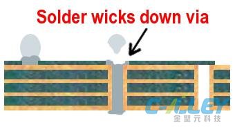
There are many reasons you shouldn’t use via-in-pad. It’s not good practice, and those via holes act like little capillary straws and suck solder off the pad or the BGA (FIGURE 1).

FIGURE 1. Capillary action can pull solder from the pad into the via.
That said, there are some applications that may require – or seem to require – via-in-pad. Here are a few examples of why you might need to use via-in-pad:
There is not enough space on the board.
It can help with thermal management.
Trace routing may be easier with via-in-pad when component spacing is tight.
High-frequency designs benefit from the shortest possible routing to bypass capacitors, which may indicate via-in-pad.
If there is no choice, here are some methods to try when using via-in-pad:
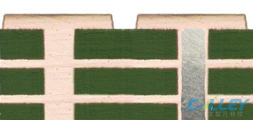
Have the board fabricator plug the via and then plate copper over it (FIGURE 2). This is our favorite option. It will give all the benefits of via-in-pad without causing problems in assembly. This is really the only via-in-pad method we recommend.
Use a microvia that goes through only one layer of the board. Although this may be an adequate option, the solder can still wander down into the via, leaving voids.
Cap the underside of the board with solder mask. This is our least favorite option because sometimes the cap can pop open, and the void may be big enough to still pull too much of the solder off the pad. Never use this method with immersion silver board finish, as outgassing inside the via can corrode the silver surface.

FIGURE 2. Capped and plugged microvia.

Please send Email to kspcba@c-alley.com or call us through +86 13828766801 Or submit your inquiry by online form. Please fill out below form and attach your manufacturing files( PCB Gerber files and BOM List) if need quotation. We will contact you shortly.
 +86 13828766801
 kspcba@c-alley.com
 https://www.kingshengpcba.com/
 2/F, Building 6, Tangtou 3rd Industrial Zone, Tangtou Community, Shiyan Town, Baoan District, Shenzhen, China, 518108