* On your first PCB Assembly order!
* Up to $300 discount
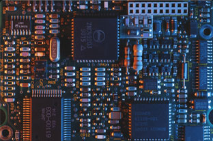
 C - A L L E Y
 About Us | Events | Company Structure | Management Staff Structure | Market Focus | Company Certification | Our Services
A variety of plated finishes are used in the PCB industry. Depending on the circuit construction and other variables, the plated finish can cause an increase in PCB insertion loss. The plated finish used on the outer ground planes of a stripline circuit have minimal or no impact on insertion loss. However, microstrip or grounded coplanar waveguide circuits, which are common on the outer layers of multilayer high-frequency PCBs, can be impacted by the plated finish for increasing the insertion loss.
In multiple experiments, comparisons were done between circuits with bare copper and circuits with different plated finishes. The bare copper circuits were used for reference only and the circuit structure was a microstrip transmission line circuit using substrates of different thickness.
The reason that most plated finishes cause increase insertion loss as compared to bare copper is that most plated finish are less conductive than copper. Electroless nickel/immersion gold (ENIG) is a very good finish. However, the simple fact is that nickel is about one-third the conductivity of copper, and a circuit with ENIG will have more insertion loss than the same circuit with bare copper. There are several variables concerning how much difference in insertion loss to expect and one of them is the substrate thickness. A substrate that is relatively thin will be more influenced by the conductor effects regarding insertion loss and the added plated finish will add to the conductor losses more for thin circuits than thick circuits. Conductor loss is one component of insertion loss.
A microstrip transmission line circuit is a simple structure with a signal conductor on the top layer and a ground plane beneath that layer. The microstrip transmission line circuit primarily has electric fields between the signal plane and ground plane, but there is a concentration of fields at the edges of the signal conductor. It is at the edges where the addition of the plated finish can increase the conductor loss, which will increase the insertion loss.
One experiment showed the difference in insertion loss of a microstrip transmission line circuit using bare copper and ENIG, but with different substrate thickness. It was found that the thinner circuits had a larger difference in insertion loss when comparing the circuits with bare copper to circuits with ENIG plated finish.
Please send Email to kspcba@c-alley.com or call us through +86 13828766801 Or submit your inquiry by online form. Please fill out below form and attach your manufacturing files( PCB Gerber files and BOM List) if need quotation. We will contact you shortly.
 +86 13828766801
 kspcba@c-alley.com
 https://www.kingshengpcba.com/
 2/F, Building 6, Tangtou 3rd Industrial Zone, Tangtou Community, Shiyan Town, Baoan District, Shenzhen, China, 518108
We would also like to thank our customers for their trust and support. The company's outstanding achievements are mainly due to the loyalty of our customers, which also encourages and spurs our company to forge ahead.


