* On your first PCB Assembly order!
* Up to $300 discount
 C - A L L E Y
About Us | Events | Company Structure | Management Staff Structure | Market Focus | Company Certification | Our Services
A new alternative using QFNs with open thermal via-in-pad (VIP) structures reduces cost and eliminates solder wicking.
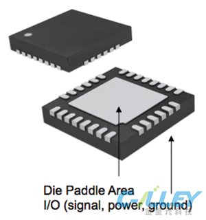
BTC packages were first offered more than 10 years ago. Since then, use has grown steadily, with a significant increase in demand observed over the past three years. BTCs are most commonly offered as QFNs (FIGURE 1). With many benefits and successful market penetration, most packaging houses now provide QFNs, albeit using different names depending on final package format, including MLF, MLPD, MLPM, MLPQ, VQFN, and DFN.

FIGURE 1. Standard QFN device bottom view.
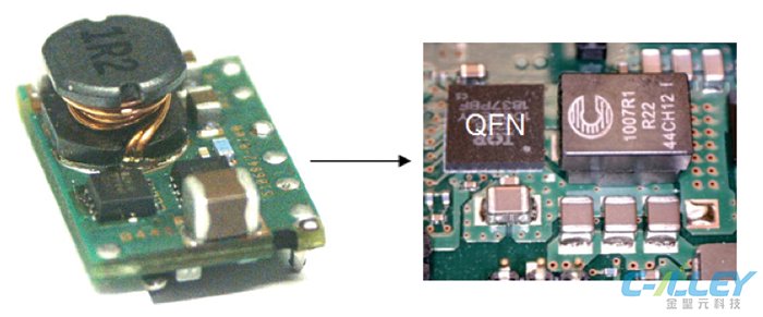
QFN packages are used to meet a variety of voltage/power regulation, logic controller, and clocking needs. The small form factor is attractive to designers looking to increase functionality using less PCB real estate. A good example is shown in FIGURE 2. Many voltage regulator designs have migrated from using a daughtercard sub-component soldered to the PCB to performing regulation directly on the main card assembly with the use of a QFN, also known as down-regulation or “down-reg.” Benefits of moving to this new layout using a QFN package within the circuit include using less PCB real estate, equivalent or increased regulation function, and simplified assembly and rework processes.


Please send Email to kspcba@c-alley.com or call us through +86 13828766801 Or submit your inquiry by online form. Please fill out below form and attach your manufacturing files( PCB Gerber files and BOM List) if need quotation. We will contact you shortly.
 +86 13828766801
 kspcba@c-alley.com
 https://www.kingshengpcba.com/
 2/F, Building 6, Tangtou 3rd Industrial Zone, Tangtou Community, Shiyan Town, Baoan District, Shenzhen, China, 518108