* On your first PCB Assembly order!
* Up to $300 discount
 C - A L L E Y
About Us | Events | Company Structure | Management Staff Structure | Market Focus | Company Certification | Our Services
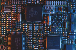
Surface mount devices, SMDs by their nature are very different to the traditional leaded components. They can be split into a number of categories:
Passive SMDs: There is quite a variety of different packages used for passive SMDs. However the majority of passive SMDs are either resistors or capacitors for which the package sizes are reasonably well standardised. Other components including coils, crystals and others tend to have more individual requirements and hence their own packages.
Resistors and capacitors have a variety of package sizes. These have designations that include: 1812, 1206, 0805, 0603, 0402, and 0201. The figures refer to the dimensions in hundreds of an inch. In other words the 1206 measures 12 hundreds by 6 hundreds of an inch. The larger sizes such as 1812 and 1206 were some of the first that were used. They are not in widespread use now as much smaller components are generally required. However they may find use in applications where larger power levels are needed or where other considerations require the larger size.
The connections to the printed circuit board are made through metallised areas at either end of the package.
Transistors and diodes: These components are often contained in a small plastic package. The connections are made via leads which emanate from the package and are bent so that they touch the board. Three leads are always used for these packages. In this way it is easy to identify which way round the device must go.
Integrated circuits: There is a variety of packages which are used for integrated circuits. The package used depends upon the level of interconnectivity required. Many chips like the simple logic chips may only require 14 or 16 pins, whereas other like the VLSI processors and associated chips can require up to 200 or more. In view of the wide variation of requirements there is a number of different packages available.
For the smaller chips, packages such as the SOIC (Small Outline Integrated Circuit) may be used. These are effectively the SMT version of the familiar DIL (Dual In Line) packages used for the familiar 74 series logic chips. Additionally there are smaller versions including TSOP (Thin Small Outline Package) and SSOP (Shrink Small Outline Package).
The VLSI chips require a different approach. Typically a package known as a quad flat pack is used. This has a square or rectangular footprint and has pins emanating on all four sides. Pins again are bent out of the package in what is termed a gull-wing formation so that they meet the board. The spacing of the pins is dependent upon the number of pins required. For some chips it may be as close as 20 thousandths of an inch. Great care is required when packaging these chips and handling them as the pins are very easily bent.
Other packages are also available. One known as a BGA (Ball Grid Array) is used in many applications. Instead of having the connections on the side of the package, they are underneath. The connection pads have balls of solder that melt during the soldering process, thereby making a good connection with the board and mechanically attaching it. As the whole of the underside of the package can be used, the pitch of the connections is wider and it is found to be much more reliable.
KingshengPCBA/C-Alley are specialized in BGA assembly. We have X-Ray for BGA testing ,and BGA rework station for repairing.
Pls contact Betty at KingshengPCBA: sales3@c-alley.com if you have Gerbers and BOM ready for quote. Or other questions are all welcome.

Please send Email to kspcba@c-alley.com or call us through +86 13828766801 Or submit your inquiry by online form. Please fill out below form and attach your manufacturing files( PCB Gerber files and BOM List) if need quotation. We will contact you shortly.
 +86 13828766801
 kspcba@c-alley.com
 https://www.kingshengpcba.com/
 2/F, Building 6, Tangtou 3rd Industrial Zone, Tangtou Community, Shiyan Town, Baoan District, Shenzhen, China, 518108