* On your first PCB Assembly order!
* Up to $300 discount
 C - A L L E Y
About Us | Events | Company Structure | Management Staff Structure | Market Focus | Company Certification | Our Services
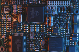
The main advantage with the HDI technique is the possibility of populating PCBs with denser BGA and QFP packages. The development of high-speed serial bus technology is pushing the signal transmission rates upwards continuously. HDI technology, with its smaller features offers reduction of several parameters to ensure higher wiring density, better electrical performance and improved signal integrity. This is especially helpful in medical equipment and other emerging product areas such as car electronics and communication base stations.
The use of thinner substrate material for prepreg in HDI technology has the advantage of improving the heat transfer across the boards. Moreover, the fabricator can select the material to have high electrical resistance but lower thermal resistance. Therefore, heat removal is more efficient from the densely packed PCBs and all components on the PCB operate within their safety zones.
With ever-increasing speeds of signals on the PCB, and the prolific use of miniature components driven by the shrinking size of electronic devices, designers and fabricators find the use of HDI techniques very helpful in fabricating advanced PCBs for achieving better features, quality, and reliability.

Please send Email to kspcba@c-alley.com or call us through +86 13828766801 Or submit your inquiry by online form. Please fill out below form and attach your manufacturing files( PCB Gerber files and BOM List) if need quotation. We will contact you shortly.
 +86 13828766801
 kspcba@c-alley.com
 https://www.kingshengpcba.com/
 2/F, Building 6, Tangtou 3rd Industrial Zone, Tangtou Community, Shiyan Town, Baoan District, Shenzhen, China, 518108