* On your first PCB Assembly order!
* Up to $300 discount
 C - A L L E Y
About Us | Events | Company Structure | Management Staff Structure | Market Focus | Company Certification | Our Services
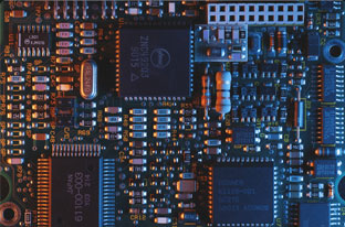
Electronic components are mechanically supported and electrically connected by printed circuit boards (PCBs), which are made of non-conductive substrate laminated with copper sheets that have conductive tracks, pads, and other characteristics etched onto them. Single-sided (one copper layer), double-sided (two copper layers), and multilayer PCBs are also available. Vias, or plated-through holes, connect conductors on various levels. Active devices, resistors, and capacitors are examples of components that can be found integrated in the substrate of an advanced PCB.
PCB copy board is also often referred to as a circuit board copy board, PCB cloning, cloning circuit board, PCB reverse engineering, etc., it refers to the kind of electronic products that have been the premise of using a variety of means to reverse the anti-product launch research PCB documents, such as a full circuit diagram technical information, and then use these data for a complete analytical product technical principles and applied research, and through the proofing system board, circuit board welding, assembly of electronic products, such as generic processes to achieve cloning process.

First, get a PCB, first record on paper all the good vitality of the model parameters, and the location, especially the direction of the diode, three machine directions of the tube, and IC notch. Preferably with a digital camera to shoot two photos vitality location.
Second, remove all the devices, and the PAD hole in the tin removed. PCB is cleaned with alcohol, and then placed in the scanner, start PHOTOSHOP, color printing mode to sweep the surface, and print them out for use.
Third, the water paper yarn and BOTTOM LAYER TOP LAYER two light sanding, polishing the shiny copper film, the scanner, start PHOTOSHOP, the two-color mode, respectively sweep. Note, PCB placed in the scanner must be horizontal tree straight, otherwise the scanned image can not be used.
Fourth, adjust canvas contrast, brightness, and contrast so that some portion of the copper film and a copper film is not strong [industrial electrical network -cnelc], and then the second drawing to black and white, check the line is clear, if not clear, repeat this step. If clear, the map in black and white BMP file format and BOT.BMP, TOP.BMP
Fifth, the two BMP file formats are converted PROTEL format files transferred in PROTEL in two basic positions coincide as over two-PAD and the VIA, indicating that the first few steps to do well, if there is deviation, the third step is repeated.
Sixth, the TOP. BMP into TOP. PCB, pay attention to the conversion to the SILK layer, that layer is yellow, and then you are in the TOP layer scanning lines it wants, and in accordance with the second step of drawing placement device. After drawing the SILK layer was deleted.
Seven, the BOT. BMP into BOT. PCB, pay attention to the conversion to the SILK layer, that layer is yellow, then you line it wants in the BOT layer description. After drawing the SILK layer was deleted.
Eight, in PROTEL in TOP. PCB and BOT. PCB is transferred and combined into a map, so the PCB copy board is complete.

Please send Email to kspcba@c-alley.com or call us through +86 13828766801 Or submit your inquiry by online form. Please fill out below form and attach your manufacturing files( PCB Gerber files and BOM List) if need quotation. We will contact you shortly.
 +86 13828766801
 kspcba@c-alley.com
 https://www.kingshengpcba.com/
 2/F, Building 6, Tangtou 3rd Industrial Zone, Tangtou Community, Shiyan Town, Baoan District, Shenzhen, China, 518108