* On your first PCB Assembly order!
* Up to $300 discount
 C - A L L E Y
About Us | Events | Company Structure | Management Staff Structure | Market Focus | Company Certification | Our Services
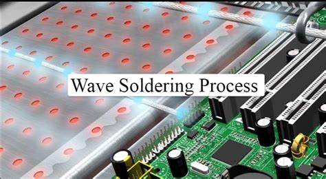
One technique for assembling electronics parts onto printed circuit boards is wave soldering. Via an incline conveyor belt, the board travels through a pot of molten solder; in the oven, the pump creates standing waves of molten solder. The components will be soldered to the PCB board as it comes into contact with the wave, resulting in joins that are both electrically and mechanically reliable. Through-hole component assembly is the main application for wave soldering, while it can also be utilized for surface mounting in rare situations.
The solder pot in the wave soldering machine is heated to the exact temperature needed for soldering. A solder wave is positioned within the tank, and the printed circuit board is passed over it until the board's bottom surface only makes contact with the solder wave.

In the process of wave solding, melted solder is transformed into required solder wave through mechanical bump or electromagnetic bump that features jet flow. Then PCBs with components assembled have to pass through solder wave so that mechanical and electric soldering between component soldering points or PCB pad.
The key steps of wave soldering contain component molding, component plug in or mounting, soldering and cooling through solder wave. It means that molded components are plugged on PCB based on requirement. Then PCB loaded with components is pushed into wave soldering system by transmission device. Next solder flux is sprayed and PCB will suffer preheating in the preheating zone. The final step comes with the wave soldering and cooling.
Components molding and plug-in components
The main job of this station is to premold some components in order to make them meet the requirements of mounting, plugging and wave soldering.
Wave soldering
The main job of wave soldering is to plug molded components on the required places according to some requirements. Then PCB loaded with components enters wave soldering system by transmission device. Soldering flux is first sprayed and PCB suffers preheating in the preheating zone. Next comes wave soldering with cooling as the final step.

Please send Email to kspcba@c-alley.com or call us through +86 13828766801 Or submit your inquiry by online form. Please fill out below form and attach your manufacturing files( PCB Gerber files and BOM List) if need quotation. We will contact you shortly.
 +86 13828766801
 kspcba@c-alley.com
 https://www.kingshengpcba.com/
 2/F, Building 6, Tangtou 3rd Industrial Zone, Tangtou Community, Shiyan Town, Baoan District, Shenzhen, China, 518108