* On your first PCB Assembly order!
* Up to $300 discount
 C - A L L E Y
About Us | Events | Company Structure | Management Staff Structure | Market Focus | Company Certification | Our Services
Testing is a crucial component of any manufacturing process operation. In the absence of thorough testing procedures, there is a chance that flaws that might lead to product failure after launch won't be found. The long-term result will be diminished consumer confidence and a bad reputation for your brand.
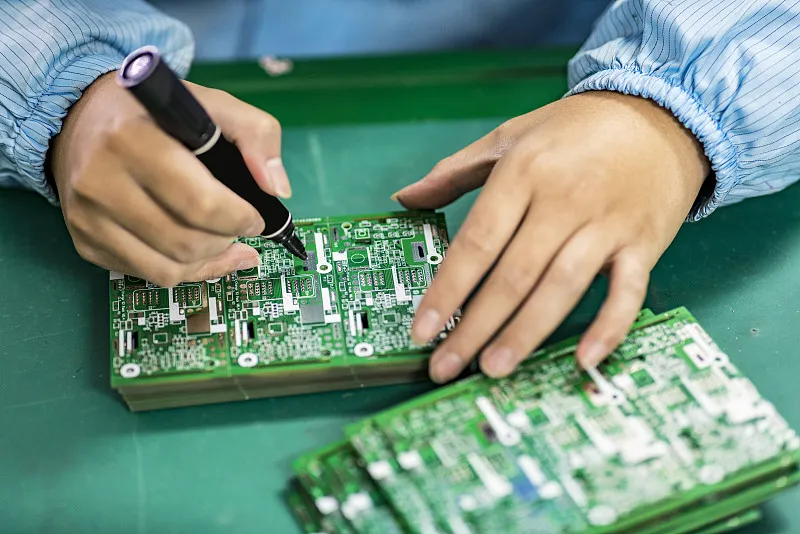
The efficient operation of electronic equipment depends on PCBs. They need to be thoroughly tested to make sure the entire device functions as intended. Testing has to be integrated into every step of the PCB design process. As part of the process, several test procedures must be carried out. Finding an error later in the development process or after the product has been out onto the market is less efficient than testing.

Testing is a crucial component of any manufacturing process operation. In the absence of thorough testing procedures, there is a chance that flaws that might lead to product failure after launch won't be found.
For PCBs, there are several test options. One common technique for providing component-level defect diagnostics is the in-circuit test (ICT) method. It is affordable and useful in discovering PCB problems prior to their integration into bigger systems. ICT is a highly precise testing method.
An analysis of manufacturing defects is carried out by specialized automated test equipment (ATE) (MDA). The testing confirms the orientation of diodes and transistors, supply voltage, passive control measurement, and each component on the PCB. It searches for short and open circuits as well. Basic functional process validation and a "vectorless" test that verifies the PCB pins are two examples of test types. Measurements that are digital and analog can be tested.
It will be necessary to get new equipment if the PCB design is altered. Consequently, the PCB needs to be made in a way that makes testing possible. One way to optimize the layout is to keep configurations simple by removing all components from the test pads.

Please send Email to kspcba@c-alley.com or call us through +86 13828766801 Or submit your inquiry by online form. Please fill out below form and attach your manufacturing files( PCB Gerber files and BOM List) if need quotation. We will contact you shortly.
 +86 13828766801
 kspcba@c-alley.com
 https://www.kingshengpcba.com/
 2/F, Building 6, Tangtou 3rd Industrial Zone, Tangtou Community, Shiyan Town, Baoan District, Shenzhen, China, 518108