* On your first PCB Assembly order!
* Up to $300 discount
 C - A L L E Y
About Us | Events | Company Structure | Management Staff Structure | Market Focus | Company Certification | Our Services
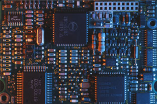
PCBs, or printed circuit boards, are the foundation of all important electronics. Almost every computational electronics device, even the more basic ones like digital clocks and calculators, uses these amazing breakthroughs. To satisfy the electrical and mechanical circuit needs of the gadget, a PCB, for the uninitiated, channels electrical impulses through electronics. To put it briefly, PCBs activate your electronics by telling the electricity where to go.
Through a system of copper channels, PCBs distribute current over their surface. Each PCB circuit board component has a specific function that is determined by the intricate network of copper routes.
Before PCB design, circuit designers are recommended to get a tour of a PC board shop and communicate with fabricators face to face over their PCB manufacturing demands. It helps prevent designers from making any unnecessary errors from getting transmitted during the design stage. However, as more companies outsource their PCB manufacturing inquiries to overseas suppliers, this becomes unpractical. Hopefully, this gives circuit designers and those new to the PCB Industry a clear view of how printed circuit boards are manufactured, and avoid making those unnecessary errors.

Process to produce a qualified pcb.
a.PCB CAM
b.Panelization
c.Copper patterning
d.Subtractive, additive and semi-additive processes
e.Chemical etching
f.Lamination
g.Drilling
h.Plating and coating
i.Solder resist application
j.Silkscreen printing
k.Bare-board test
l.Assembly
m.Protection and packaging

Please send Email to kspcba@c-alley.com or call us through +86 13828766801 Or submit your inquiry by online form. Please fill out below form and attach your manufacturing files( PCB Gerber files and BOM List) if need quotation. We will contact you shortly.
 +86 13828766801
 kspcba@c-alley.com
 https://www.kingshengpcba.com/
 2/F, Building 6, Tangtou 3rd Industrial Zone, Tangtou Community, Shiyan Town, Baoan District, Shenzhen, China, 518108