* On your first PCB Assembly order!
* Up to $300 discount
 C - A L L E Y
About Us | Events | Company Structure | Management Staff Structure | Market Focus | Company Certification | Our Services
Printed circuit board (PCB) is one of the most common names, and can also be called "printed wiring boards" or "printed wiring cards". Before the PCB appeared, the circuit was made up of point-to-point wiring. The reliability of this method is very low, because as the circuit ages, the breakage of the line can cause an open or short circuit of the line node.
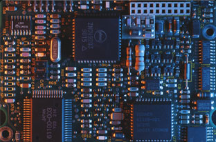
Copper traces, pads, and conductive planes are examples of conductive structures found on printed circuit boards. An insulating material is layered between conductor layers to form the mechanical structure. A silk screen material is printed on top of the non-conductive solder mask, which covers the entire structure and serves as a legend for the electronic components. Following these fabrication stages, the printed circuit board assembly receives the bare board, which is then used to solder components to the board and test the PCBA.
Within the electronics business, printed circuit board design has developed into a distinct vertical. PCBs are crucial because they offer sturdy support for holding components in place, electrical connections between components, and a small packaging that can be integrated into a finished device. The greatest software can assist in taking a design from concept to manufacture. Even the most basic circuit board requires careful design utilizing specialized software tools. We'll delve deeper into the definition of a printed circuit board (PCB), its design, and some key concepts to grasp when creating circuit boards in this post.
Winding technology is a major advancement in circuit technology that enhances the durability and replaceability of the line by winding small diameter wires around the posts at the joint.
As the electronics industry evolved from vacuum tubes and relays to silicon semiconductors and integrated circuits, the size of electronic components has decreased and prices have fallen. Electronic products are appearing more and more frequently in the consumer sector, prompting manufacturers to look for smaller and more cost-effective solutions. So, the PCB was born.
Kingsheng PCBA provides both PCB and PCB assembly services.

Component packaging, which is used to house semiconductor chips in integrated circuits (ICs), is the next generation of PCB components. Modern processors and digital/RF modules use chips that are positioned on an IC substrate to connect the electrical contacts on the die to the PCB. These parts are used in integrated circuits, yet they resemble miniature circuit boards in essence and can even be designed using PCB design tools. For instance, the bottom side of an earlier CPU is depicted in the image below, but the supporting parts on the IC substrate are visible from the bottom side.

Please send Email to kspcba@c-alley.com or call us through +86 13828766801 Or submit your inquiry by online form. Please fill out below form and attach your manufacturing files( PCB Gerber files and BOM List) if need quotation. We will contact you shortly.
 +86 13828766801
 kspcba@c-alley.com
 https://www.kingshengpcba.com/
 2/F, Building 6, Tangtou 3rd Industrial Zone, Tangtou Community, Shiyan Town, Baoan District, Shenzhen, China, 518108