* On your first PCB Assembly order!
* Up to $300 discount
 C - A L L E Y
About Us | Events | Company Structure | Management Staff Structure | Market Focus | Company Certification | Our Services
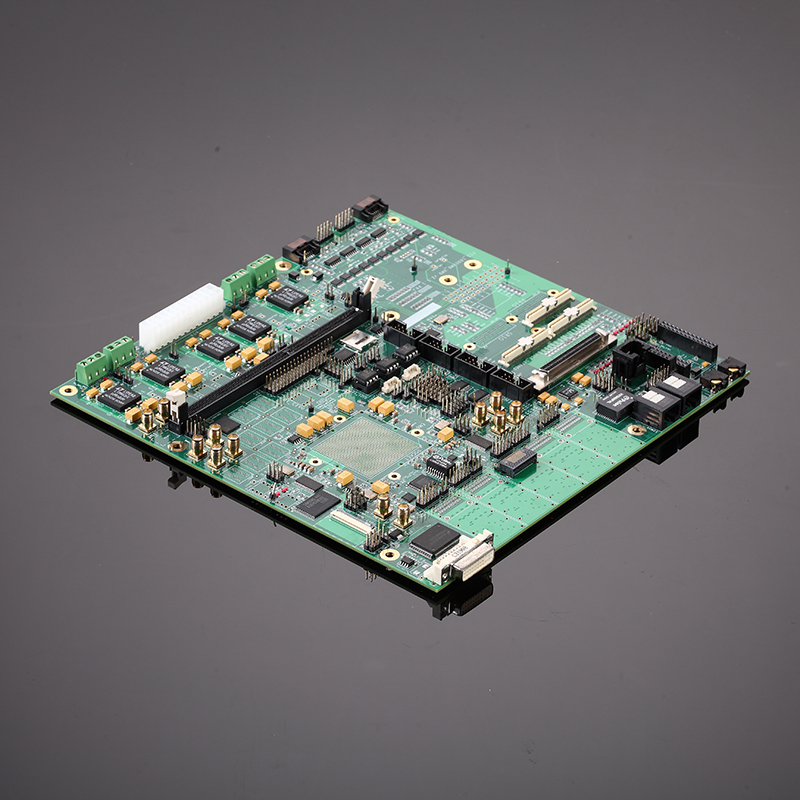
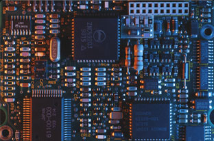
The Printed Circuit Boards (PCBs) are the main structural component of modern electronics. The amazing creation has made it possible for electronics of all kinds to advance. A PCB serves as a conduit for current flow via its copper route and heat dissipation mechanism, maintaining the minuscule yet intricate electronic devices in optimal working order.
ICs, transformers, transmitters, and other electronic parts are organized on the PCBs. The PCB is referred to as the PCBA once these components are installed on it. Therefore, the steps of solder paste, component choosing and positioning, soldering, and final inspection come next in the PCBA production process.
You need to be well-versed in the PCB assembly process if you want to get the best PCBA and PCB for your electronic devices.
1. PCB size
The size of the PCB is limited by the capabilities of the electronic processing production line equipment. Therefore, the appropriate PCB size should be considered when designing the product system scheme.
2. PCB shape
SMT production equipment uses guide rails to transport PCBs, and cannot transport PCBs with irregular shapes, especially PCBs with gaps in the corners.
3. Transmission side
The size of the conveying edge depends on the requirements of the conveying rail of the equipment, printing presses, placement machines and reflow soldering furnaces generally require the conveying edge to be above 3.5mm.
4. Positioning hole
Many processes such as imposition processing, assembly, and testing require accurate positioning of the PCB. Therefore, positioning holes are generally required to be designed.
5. Positioning symbol
Modern placement machines, printing machines, optical inspection equipment (AOI), solder paste inspection equipment (SPI), etc. all use optical positioning systems. Therefore, optical positioning symbols must be designed on the PCB.

Due to the intricate and technical nature of PCB assembly, many factors must be carefully considered, and even minor adjustments can have a significant impact on the final cost and quality of the product. This article's descriptions of the PCB assembly process only focus on standard PCBA practices and technologies. Design files and client requirements have a major role in determining and influencing the actual manufacturing process. Therefore, before placing a PCBA order, consumers must carefully consider how to evaluate a reputable PCB assembler.

Please send Email to kspcba@c-alley.com or call us through +86 13828766801 Or submit your inquiry by online form. Please fill out below form and attach your manufacturing files( PCB Gerber files and BOM List) if need quotation. We will contact you shortly.
 +86 13828766801
 kspcba@c-alley.com
 https://www.kingshengpcba.com/
 2/F, Building 6, Tangtou 3rd Industrial Zone, Tangtou Community, Shiyan Town, Baoan District, Shenzhen, China, 518108