* On your first PCB Assembly order!
* Up to $300 discount
 C - A L L E Y
About Us | Events | Company Structure | Management Staff Structure | Market Focus | Company Certification | Our Services
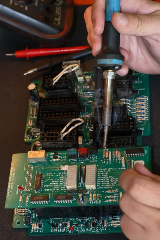
PCB designers are responsible for designing the technology that powers our modern electronics. They have to balance a host of requirements and navigate a complex layout that is as much art as it is science. However, even the most carefully designed printed circuit boards can face defects during PCB fabrication and assembly. In this blog, we will provide an overview of the most common assembly defects - some that PCB design can influence, and some that are related specifically to the assembly process itself.
It’s the goal of all SMT assemblers to minimize all solder joint defects. Only through understanding of defect root causes, and their prevention can improvements in product quality be realized and sustained. Open Solder Joints occur when there is a lack of an integral bond between the component lead and PCB pad, or other point of connection on a PCB. These types of defects can occur when solder appears only on the PCB pad while not on the component lead (or vice versa).
1. PCB component shift
The misalignment of a component with its target is called "component shift". It occurs during the reflow phase, where components may float on the molten solder, causing realignment.
However, preventive measures can be taken to avoid this situation. It includes following the required humidity and temperature (also called reflow profile), and improving the accuracy of the components in the SMT placement machine. You can also reduce the amount of component movement and use aggressive flux to improve the solderability of the PCB to prevent defects.
2. Corrosion caused by flux residue
Flux is usually used before soldering to reduce oxides formed on the copper surface. However, the problem with this is that because it contains corrosive components, such as chlorine or bromine, it can cause surface corrosion.
Corrosion can be prevented by removing flux residues when cleaning the wave soldering tray. When cleaning the residue, please use the same solvent as the diluted flux and fiber-free cloth to prevent the debris from contaminating other products.

The failure of a Printed Circuit Board Assembly (PCBA) largely depends on whether it is classified as a class 2 or class 3 product. According to IPC standards, class 2 products are expected to function for an extended period of time while maintaining a decent level of performance, but they don't need to function continuously. On the other hand, class 3 products require high and consistent performance at all times, and any downtime is unacceptable. Class 3 products may also need to operate in harsh environments and critical systems, such as life support. To avoid any latent failures, it is essential to ensure that each assembly is of the highest quality and in proper working condition before leaving our shop.

Please send Email to kspcba@c-alley.com or call us through +86 13828766801 Or submit your inquiry by online form. Please fill out below form and attach your manufacturing files( PCB Gerber files and BOM List) if need quotation. We will contact you shortly.
 +86 13828766801
 kspcba@c-alley.com
 https://www.kingshengpcba.com/
 2/F, Building 6, Tangtou 3rd Industrial Zone, Tangtou Community, Shiyan Town, Baoan District, Shenzhen, China, 518108