
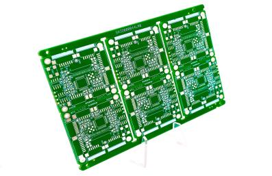
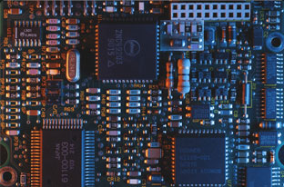
04-11 | Industry
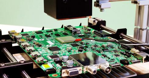
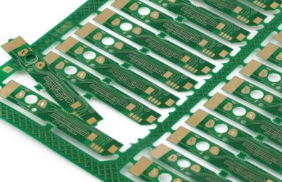
The size of a printed circuit board (PCB) is limited by the capabilities of the electronic processing production line equipment. Therefore, it is essential to consider the appropriate PCB size during product design.
03-22 | Industry
During the PCBA (Printed Circuit Board Assembly) processing, factors related to the manufacturing process and manual operations can lead to the occurrence of solder beads and dross on the PCBA board. These issues pose significant risks, as loose ...
03-22 | Industry
Bubbles are typically generated during the reflow and wave soldering processes in SMT chip manufacturing. These bubbles can not only detract from the visual appeal of the PCBA but also compromise the overall quality of the products. To prevent solder.
03-22 | Industry
While it is normal for the placement machine to experience some PCBA rejection, a high rate of such incidents can significantly affect production efficiency and costs. If there is a serious issue with PCBA rejection, consult on-site personnel and...
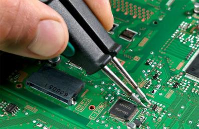
03-22 | Industry
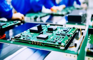
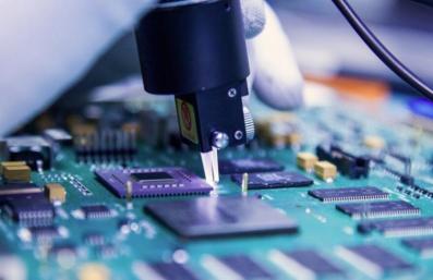
SMT (Surface Mount Technology) welding is a vital part of the assembly process for electronic devices. Without proper quality assurance in the SMT welding process, even the best-designed electronic equipment may fail to meet its design objectives.
03-22 | Industry
The process of copying a printed circuit board (PCB) involves several straightforward steps. First, you scan the PCB that needs to be copied and record the precise positions of the components. After that, disassemble the components to create a bill of
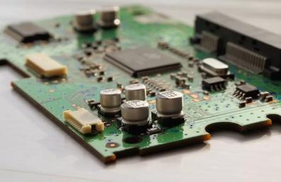
03-08 | Industry
The Failure Mechanisms of Components on PCBA Boards: An In-depth Analysis. Electrolytic capacitors and certain types of film capacitors are susceptible to failure due to chemical reactions within their dielectrics, which can be initiated by trace ...
03-08 | Industry
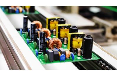
Key Points of Power Supply Design for RF Circuits: The power cord is an important pathway for EMI (Electromagnetic Interference) access to the circuit. Through the power line, external interference can be transmitted to the internal circuit...
03-08 | Industry
Depending on the actual usage environment and intended purpose of the product, the testing is generally categorized into several types, including: - Withstand Voltage Test - Insulation Test - Salt Spray Test - Impedance Test - Vibration Test ...
03-08 | Industry
PCB splicing is primarily done for production convenience. In a plate factory, the base material is typically large, allowing for multiple boards to be manufactured simultaneously and then cut individually. If splicing is mainly utilized for welding..
03-08 | Industry
Understanding the insertion of electronic components on a PCB (Printed Circuit Board) is crucial for electronic engineers. The process of inserting components is quite detailed and involves several key principles. This guide outlines the methods and
02-24 | Industry
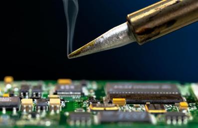
Lead is a toxic substance, and excessive absorption of lead by the human body can cause lead poisoning. Even low-dose intake can negatively affect human intelligence, the nervous system, and the reproductive system. An alloy of tin and lead is...
We would also like to thank our customers for their trust and support. The company's outstanding achievements are mainly due to the loyalty of our customers, which also encourages and spurs our company to forge ahead.